HD74HC4543 View Datasheet(PDF) - Renesas Electronics
Part Name
Description
MFG CO.
HD74HC4543 Datasheet PDF : 9 Pages
| |||
HD74HC4543
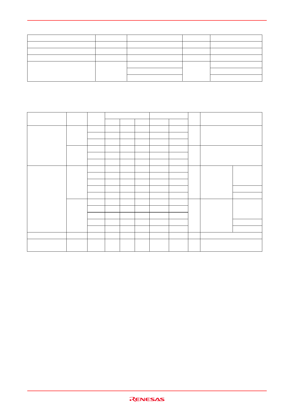
Recommended Operating Conditions
Item
Symbol
Ratings
Supply voltage
VCC
2 to 6
Input / Output voltage
VIN, VOUT
0 to VCC
Operating temperature
Ta
–40 to 85
Input rise / fall time*1
0 to 1000
tr, tf
0 to 500
0 to 400
Note: 1. This item guarantees maximum limit when one input switches.
Waveform: Refer to test circuit of switching characteristics.
Unit
V
V
°C
ns
Conditions
VCC = 2.0 V
VCC = 4.5 V
VCC = 6.0 V
Electrical Characteristics
Item
Input voltage
Output voltage
Input current
Quiescent supply
current
Symbol
VIH
VIL
VOH
VOL
Iin
ICC
VCC (V)
2.0
4.5
6.0
2.0
4.5
6.0
2.0
4.5
6.0
4.5
6.0
2.0
4.5
6.0
4.5
6.0
6.0
6.0
Ta = 25°C
Min Typ Max
1.5 — —
3.15 — —
4.2 — —
— — 0.5
— — 1.35
— — 1.8
1.9 2.0 —
4.4 4.5 —
5.9 6.0 —
4.18 — —
5.68 — —
— 0.0 0.1
— 0.0 0.1
— 0.0 0.1
— — 0.26
— — 0.26
— — ±0.1
— — 4.0
Ta = –40 to+85°C
Min Max Unit
Test Conditions
1.5
—
V
3.15
—
4.2
—
—
0.5 V
—
1.35
—
1.8
1.9
—
V Vin = VIH or VIL IOH = –20 µA
4.4
—
5.9
—
4.13
—
IOH = –4 mA
5.63
—
IOH = –5.2 mA
—
0.1
V Vin = VIH or VIL IOL = 20 µA
—
0.1
—
0.1
—
0.33
IOH = 4 mA
—
0.33
IOH = 5.2 mA
—
±1.0 µA Vin = VCC or GND
—
40 µA Vin = VCC or GND, Iout = 0 µA
Rev.2.00 Mar 30, 2006 page 4 of 8
Share Link: 