IRF540NPBF View Datasheet(PDF) - International Rectifier
Part Name
Description
MFG CO.
IRF540NPBF Datasheet PDF : 9 Pages
| |||
IRF540NPbF
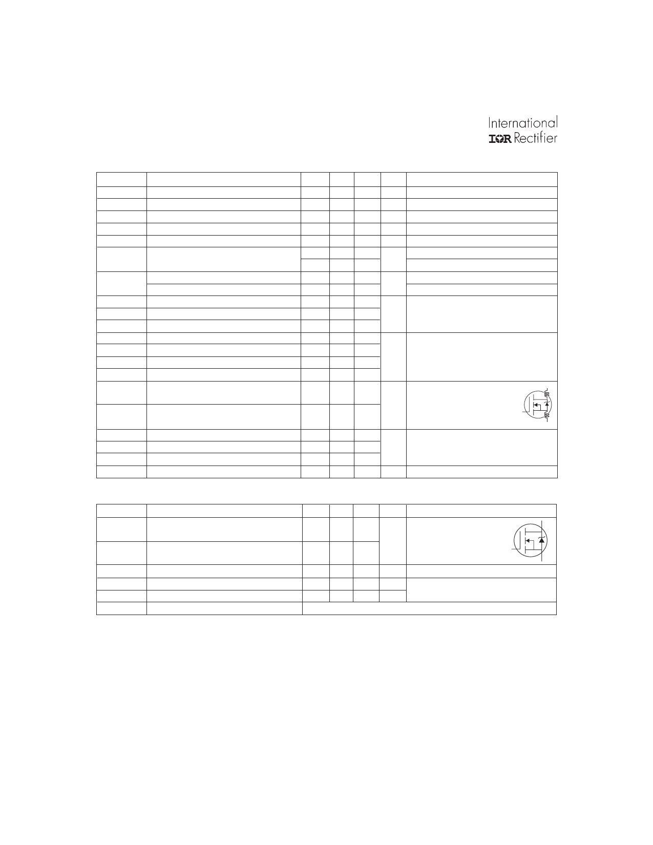
Electrical Characteristics @ TJ = 25°C (unless otherwise specified)
V(BR)DSS
∆V(BR)DSS/∆TJ
RDS(on)
VGS(th)
gfs
Parameter
Drain-to-Source Breakdown Voltage
Breakdown Voltage Temp. Coefficient
Static Drain-to-Source On-Resistance
Gate Threshold Voltage
Forward Transconductance
IDSS
Drain-to-Source Leakage Current
IGSS
Qg
Qgs
Qgd
td(on)
tr
td(off)
tf
Gate-to-Source Forward Leakage
Gate-to-Source Reverse Leakage
Total Gate Charge
Gate-to-Source Charge
Gate-to-Drain ("Miller") Charge
Turn-On Delay Time
Rise Time
Turn-Off Delay Time
Fall Time
LD
Internal Drain Inductance
LS
Internal Source Inductance
Ciss
Input Capacitance
Coss
Output Capacitance
Crss
Reverse Transfer Capacitance
EAS
Single Pulse Avalanche Energy
Min. Typ. Max. Units
Conditions
100 ––– ––– V VGS = 0V, ID = 250µA
––– 0.12 ––– V/°C Reference to 25°C, ID = 1mA
––– ––– 44 mΩ VGS = 10V, ID = 16A
2.0 ––– 4.0 V VDS = VGS, ID = 250µA
21 ––– ––– S VDS = 50V, ID = 16A
––– ––– 25
––– ––– 250
µA VDS = 100V, VGS = 0V
VDS = 80V, VGS = 0V, TJ = 150°C
––– ––– 100 nA VGS = 20V
––– ––– -100
VGS = -20V
––– ––– 71
ID = 16A
––– ––– 14 nC VDS = 80V
––– ––– 21
––– 11 –––
VGS = 10V, See Fig. 6 and 13
VDD = 50V
––– 35 ––– ns ID = 16A
––– 39 –––
RG = 5.1Ω
––– 35 –––
VGS = 10V, See Fig. 10
Between lead,
D
––– 4.5 –––
6mm (0.25in.)
nH from package
G
––– 7.5 –––
and center of die contact
S
––– 1960 –––
VGS = 0V
––– 250 –––
VDS = 25V
––– 40 ––– pF ƒ = 1.0MHz, See Fig. 5
––– 700 185 mJ IAS = 16A, L = 1.5mH
Source-Drain Ratings and Characteristics
Parameter
IS
Continuous Source Current
(Body Diode)
ISM
Pulsed Source Current
(Body Diode)
VSD
Diode Forward Voltage
trr
Reverse Recovery Time
Qrr
Reverse Recovery Charge
ton
Forward Turn-On Time
Notes:
Repetitive rating; pulse width limited by
max. junction temperature. (See fig. 11)
Starting TJ = 25°C, L =1.5mH
RG = 25Ω, IAS = 16A. (See Figure 12)
Min. Typ. Max. Units
Conditions
MOSFET symbol
D
––– ––– 33
A showing the
integral reverse
G
––– ––– 110
p-n junction diode.
S
––– ––– 1.2 V TJ = 25°C, IS = 16A, VGS = 0V
––– 115 170 ns TJ = 25°C, IF = 16A
––– 505 760 nC di/dt = 100A/µs
Intrinsic turn-on time is negligible (turn-on is dominated by LS+LD)
ISD ≤ 16A, di/dt ≤ 340A/µs, VDD ≤ V(BR)DSS,
TJ ≤ 175°C
Pulse width ≤ 400µs; duty cycle ≤ 2%.
This is a typical value at device destruction and represents
operation outside rated limits.
This is a calculated value limited to TJ = 175°C .
2
www.irf.com
Share Link: 