AD53040KRP View Datasheet(PDF) - Analog Devices
Part Name
Description
MFG CO.
AD53040KRP Datasheet PDF : 7 Pages
| |||
AD53040
APPLICATION INFORMATION
Power Supply Distribution, Bypassing and Sequencing
The AD53040 draws substantial transient currents from its
power supplies when switching between states and careful design
of the power distribution and bypassing is key to obtaining speci-
fied performance. Supplies should be distributed using broad,
low inductance traces or (preferably) planes in a multilayered
board with a dedicated ground-plane layer. All of the device’s
power supply pins should be used to minimize the internal in-
ductance presented by the part’s bond wires. Each supply must
be bypassed to ground with at least one 0.1 µF capacitor; chip-
style capacitors are preferable as they minimize inductance. One
or more 10 µF (or greater) Tantalum capacitors per board are
also advisable to provide additional local energy storage.
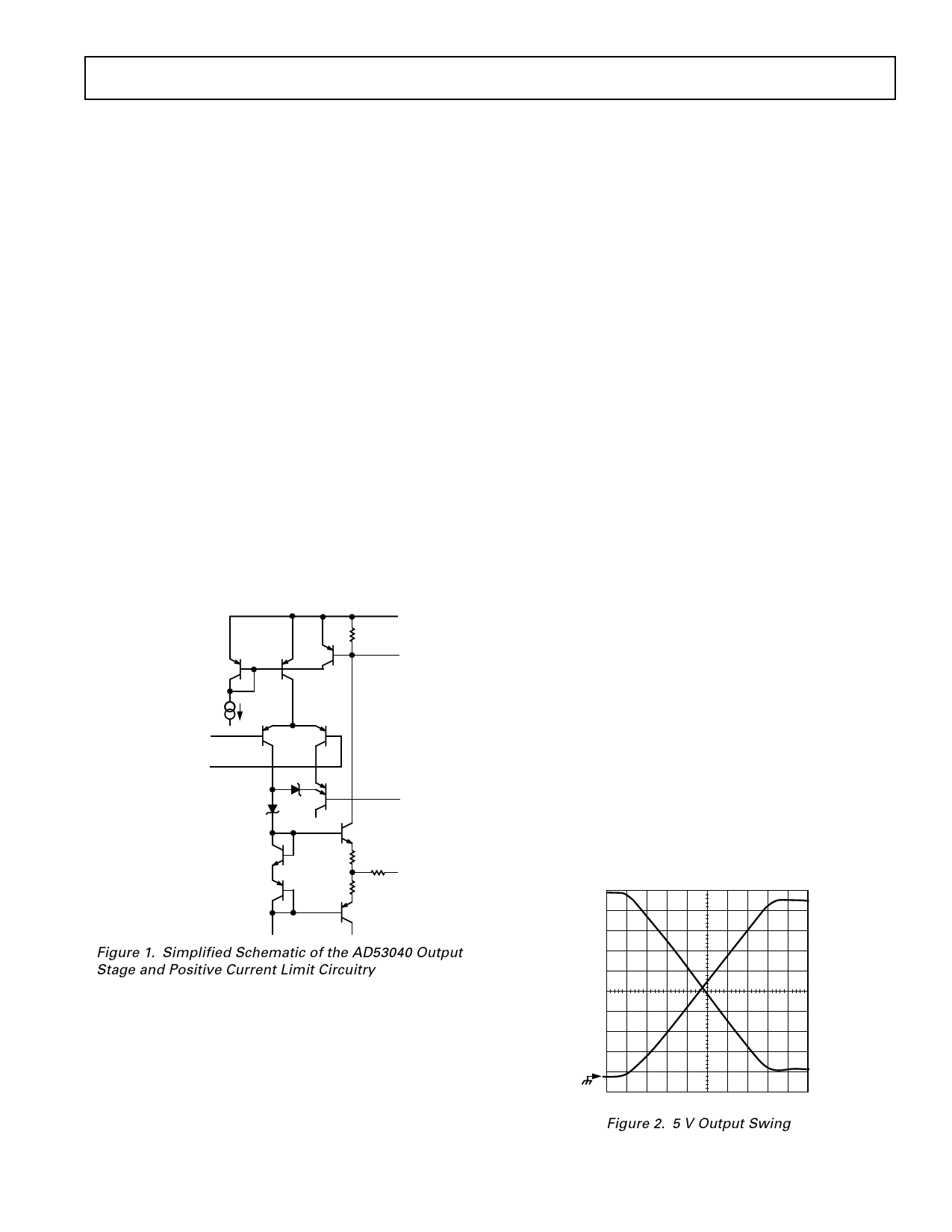
The AD53040’s current-limit circuitry also requires external
bypass capacitors. Figure 1 shows a simplified schematic of the
positive current-limit circuit. Excessive collector current in out-
put transistor Q49 creates a voltage drop across the 10 Ω resis-
tor, which turns on PNP transistor Q48. Q48 diverts the rising-
edge slew current, shutting down the current mirror and remov-
ing the output stage’s base drive. The VHDCPL pin should be
bypassed to the positive supply with a 0.039 µF capacitor, while
the VLDCPL pin (not shown) requires a similar capacitor to the
negative supply- these capacitors ensure that the AD53040
doesn’t current limit during normal output transitions up the its
full 9 V rated step size. Both capacitors must have minimum-
length connections to the AD53040. Here again, chip capacitors
are ideal.
VPOS
10⍀؎10%
Q48
VHDCPL
RISING-EDGE SLEW
CONTROL CURRENT
LEVEL-SHIFTED
LOGIC DRIVE
VH
VNEG
Q49
Several points about the current-limit circuitry should be noted.
First, the limiting currents are not tightly controlled, as they are
functions of both absolute transistor VBES and junction tem-
perature; higher dc output current is available at lower junction
temperatures. Second, it is essential to connect the VHDCPL
capacitor to the positive supply (and the VLDCPL capacitor to
the negative supply)—failure to do so causes considerable ther-
mal stress in the current-limiting resistor(s) during normal sup-
ply sequencing and may ultimately cause them to fail, rendering
the part nonfunctional. Finally, the AD53040 may appear to
function normally for small output steps (less than 3 V or so) if
one or both of these capacitors is absent, but it will exhibit
excessive rise or fall times for steps of larger amplitude.
The AD53040 does not require special power-supply sequencing.
However, good design practice dictates that digital and analog
control signals not be applied to the part before the supplies are
stable. Violating this guideline will not normally destroy the
part, but the active inputs can draw considerable current until
the main supplies are applied.
Digital Input Range Restrictions
Total range amongst all digital signals (DATA, DATA, INH,
and INH) has to be less than or equal to 2 V to meet specified
timing. The device will function above 2 V with reduced perfor-
mance up to the absolute maximum limit. This performance
degradation might not be noticed in all modes of operation. Of
all the six possible transitions (VH v VL, VL v VH, VH v INH,
INH v VH, VL v INH and INH v VL), there may be only one
that would show a degradation, usually in delay time. Taken to
the extreme, the driver may fail to achieve a proper output volt-
age, output impedance or may fail to fully inhibit.
An example of a scenario that would not work for the AD53040
is if the part is driven using 5 V single-ended CMOS. One pin of
each differential input would be tied to a +2.5 V reference level
and the logic voltages would be applied to the other. This would
meet the Absolute Maximum Rating of ± 3 V because the max
differential is ± 2.5 V. It is however possible, for example for
0.0 V to be applied to the INH input and +5 V to be applied to
the DATA input. This 5 V difference far exceeds the 2.0 V
limitation given above. Even using 3 V CMOS or TTL the
difference between logic high and logic low is greater than or
equal to 3 V which will not properly work. The only solution is
to use resistive dividers or equivalent to reduce the voltage levels.
OUT
Q50
Figure 1. Simplified Schematic of the AD53040 Output
Stage and Positive Current Limit Circuitry
5.12V
550mV
/DIV
REV. B
–380mV
66.25ns
500ps/DIV
71.25ns
Figure 2. 5 V Output Swing
–5–
Share Link: 