HEF4541BP,652 View Datasheet(PDF) - NXP Semiconductors.
Part Name
Description
MFG CO.
HEF4541BP,652 Datasheet PDF : 17 Pages
| |||
NXP Semiconductors
HEF4541B
Programmable timer
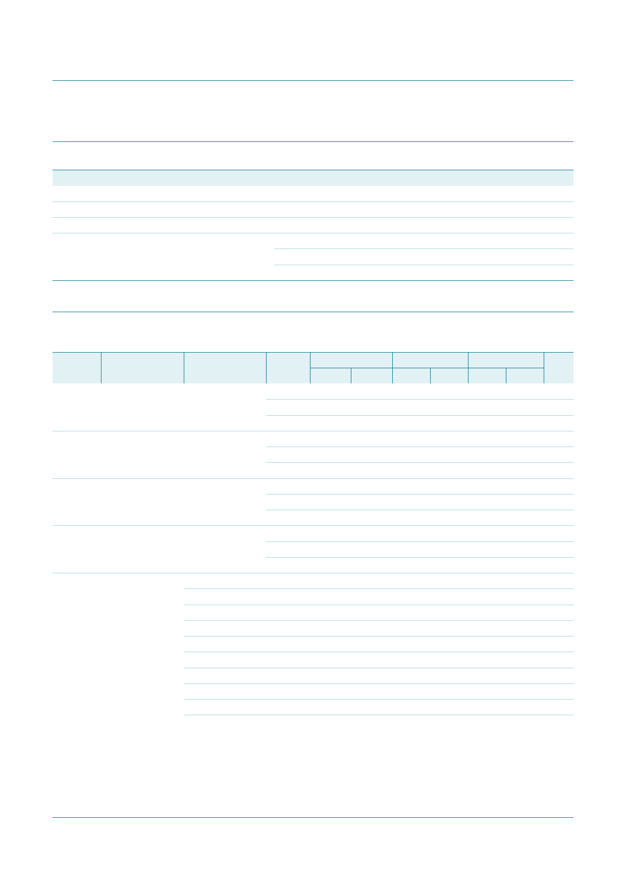
8. Recommended operating conditions
Table 6.
Symbol
VDD
VI
Tamb
Δt/ΔV
Recommended operating conditions
Parameter
Conditions
supply voltage
input voltage
ambient temperature
in free air
input transition rise and fall rate
VDD = 5 V
VDD = 10 V
VDD = 15 V
9. Static characteristics
Min Max
3
15
0
VDD
−40
+85
-
3.75
-
0.5
-
0.08
Unit
V
V
°C
μs/V
μs/V
μs/V
Table 7. Static characteristics
VSS = 0 V; VI = VSS or VDD; unless otherwise specified.
Symbol Parameter
Conditions
VDD
VIH
HIGH-level
|IO| < 1 μA
input voltage
5V
10 V
15 V
VIL
LOW-level
|IO| < 1 μA
input voltage
5V
10 V
15 V
VOH
HIGH-level
|IO| < 1 μA
output voltage
5V
10 V
15 V
VOL
LOW-level
|IO| < 1 μA
output voltage
5V
10 V
15 V
IOH
HIGH-level
CTC, RTC;
output current
VO = 2.5 V
5V
VO = 4.6 V
5V
VO = 9.5 V
10 V
VO = 13.5 V
15 V
O;
VO = 2.5 V
VO = 4.6 V
VO = 9.5 V
VO = 13.5 V
5V
5V
10 V
15 V
Tamb = −40 °C
Min Max
3.5
-
7.0
-
11.0
-
-
1.5
-
3.0
-
4.0
4.95
-
9.95
-
14.95
-
-
0.05
-
0.05
-
0.05
Tamb = 25 °C
Min Max
3.5
-
7.0
-
11.0
-
-
1.5
-
3.0
-
4.0
4.95
-
9.95
-
14.95
-
-
0.05
-
0.05
-
0.05
Tamb = 85 °C Unit
Min Max
3.5
-V
7.0
-V
11.0
-V
-
1.5 V
-
3.0 V
-
4.0 V
4.95
-V
9.95
-V
14.95
-V
-
0.05 V
-
0.05 V
-
0.05 V
-
−1.4
-
−1.2
-
−0.95 mA
-
−0.5
-
−0.4
-
−0.3 mA
-
−1.4
-
−1.2
-
−0.95 mA
-
−4.8
-
−4.0
-
−3.2 mA
-
−1.7
-
−1.4
-
−1.1 mA
-
−0.64
-
−0.5
-
−0.36 mA
-
−1.6
-
−1.3
-
−0.9 mA
-
−4.2
-
−3.4
-
−2.4 mA
HEF4541B
Product data sheet
All information provided in this document is subject to legal disclaimers.
Rev. 4 — 25 June 2012
© NXP B.V. 2012. All rights reserved.
5 of 17
Share Link: 