AD8321(Rev0) View Datasheet(PDF) - Analog Devices
Part Name
Description
MFG CO.
AD8321 Datasheet PDF : 19 Pages
| |||
AD8321
OPERATIONAL DESCRIPTION
The AD8321 is a digitally controlled variable gain power ampli-
fier that is optimized for driving a 75 Ω cable. As a multifunc-
tional bipolar device on a single silicon die, it incorporates all
the analog features necessary to accommodate reverse path
(upstream) high speed (5 MHz to 65 MHz) cable data modem
requirements. The AD8321 has an overall gain range of ap-
proximately 53 dB and is capable of greater than 100 MHz
operation at output signal levels exceeding 12 dBm. Overall,
when considering the device’s wide gain range, low distortion,
wide bandwidth and variable load drive, the device can be used
in many variable gain block applications.
VCC
GND
VIN+
VIN–
AD8321
INV
ATTENUATOR CORE
PWR
AMP
REVERSE
AMP
VOUT
DATADASTHAIFLTARTECGHISTER
POWER-
DOWN/
PD
SWITCH
DATA SHIFT REGISTER
INTER
DATEN CLK
SDATA
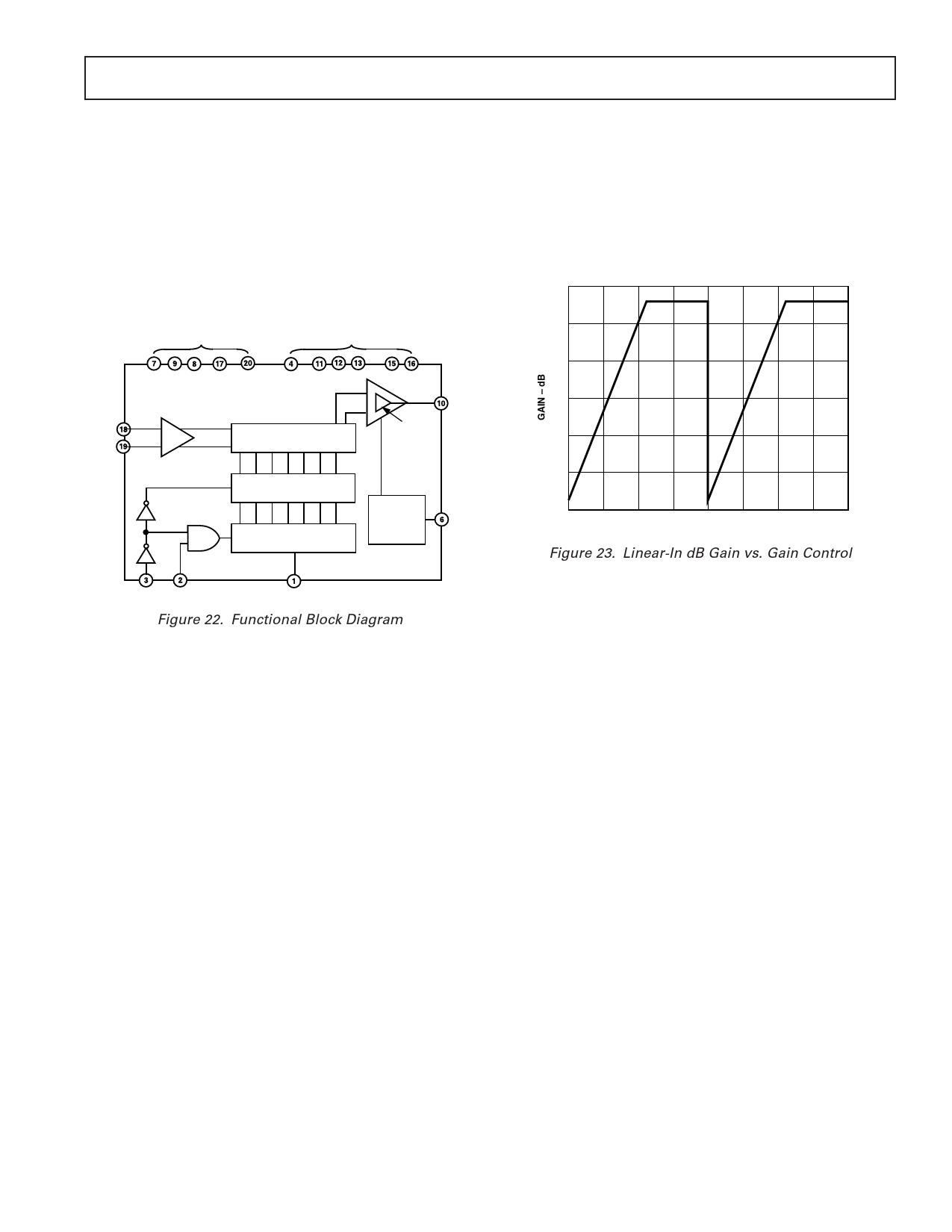
Figure 22. Functional Block Diagram
The digitally programmable gain is controlled by the three-wire
“SPI” compatible inputs. These inputs are called SDATA
(serial data input port), DATEN (data enable low input port)
and CLK (clock input port). See Pin Function Descriptions
and Functional Block diagram. The AD8321 is programmed by
an 8-bit “attenuator” word. When a standard 8-bit word is
used, the first data bit MSB will be shifted out of the 7-bit shift
register during the eighth rising CLK edge. The lower seven
bits will then be loaded into the AD8321’s digital decode sec-
tion when the DATEN input is taken high.
The gain of the AD8321 is linear in steps of 0.7526 dB. The
gain transfer function starts at –27.43 dB (at decimal code 0)
and increases 0.7526 dB/LSB. The gain increases up to decimal
code 71. At this point the gain is at its maximum level of 26 dB.
If a decimal word between 71 and 127 is entered, the gain is no
longer incremented and stays at 26 dB. Since the MSB of an 8-bit
word is a “don’t care” bit, at decimal code 128, the AD8321’s
gain returns to its minimum value. The gain vs. gain control
relationship repeats itself as shown in Figure 23 for the upper
127 codes.
The gain transfer function is as follows:
AV = 26 dB – ((71 – CODE) × 0.7526 dB) for CODE ≤ 71
AV = 26 dB for 71 ≤ CODE ≤ 127
AV = 26 dB + ((199 – CODE) × 0.7526 dB) for 128 ≤
CODE ≤ 199
AV = 26 dB for 199 ≤ CODE ≤ 255
where CODE is the decimal equivalent of the 8-bit word loaded in
the AD8321’s data latch (see Figure 23).
30
20
10
0
–10
–20
–30
0
32
64
96 128 160 192 224 256
GAIN CODE – Decimal
Figure 23. Linear-In dB Gain vs. Gain Control
The AD8321 is composed of four analog functions in the
power-up or forward mode. The input amplifier (preamp) which
can be used single-endedly or differentially and provides a maxi-
mum of 12 dB of attenuation. If the input is used in the differ-
ential configuration, it is imperative that the input signals are
180 degrees out of phase and of equal amplitudes. This will
ensure the proper gain accuracy and harmonic performance.
The preamp stage drives a vernier stage that provides the fine
tune gain adjustment. The 0.7526 dB step resolution is imple-
mented in this stage. After the vernier stage, a DAC provides the
bulk of the AD8321’s attenuation (six bits or 36 dB). The signals
in the preamp and vernier gain blocks are differential to im-
prove the PSRR and linearity. A single-ended current is fed
from the DAC into the output stage, which amplifies this cur-
rent to the appropriate level necessary to drive a 75 Ω load. The
output stage utilizes negative feedback to implement a
75 Ω output impedance. This eliminates the need for an exter-
nal 75 Ω matching resistor needed in typical video (or video
filter) termination requirements.
REV. 0
–7–
Share Link: 