MJ15024 View Datasheet(PDF) - ON Semiconductor
Part Name
Description
MFG CO.
MJ15024 Datasheet PDF : 4 Pages
| |||
NPN − MJ15022, MJ15024*
ÎÎÎÎÎÎÎÎÎÎÎÎÎÎÎÎÎÎÎÎÎÎÎÎÎÎÎÎÎÎÎÎÎ ELECTRICAL CHARACTERISTICS (TC = 25_C unless otherwise noted)
ÎÎÎÎÎÎÎÎÎÎÎÎÎÎÎÎÎÎÎÎÎÎÎÎÎÎÎÎÎÎÎÎÎ Characteristic
Symbol
Min
ÎÎÎÎÎÎÎÎÎÎÎÎÎÎÎÎÎÎÎÎÎÎÎÎÎÎÎÎÎÎÎÎÎ OFF CHARACTERISTICS
ÎÎÎÎÎÎÎÎÎÎÎÎÎÎÎÎÎÎÎÎÎÎÎÎÎÎÎÎÎÎÎÎÎ Collector−Emitter Sustaining Voltage (Note 2)
ÎÎÎÎÎÎÎÎÎÎÎÎÎÎÎÎÎÎÎÎÎÎÎÎÎÎÎÎÎÎÎÎÎ (IC = 100 mAdc, IB = 0)
VCEO(sus)
MJ15022
200
MJ15024
250
ÎÎÎÎÎÎÎÎÎÎÎÎÎÎÎÎÎÎÎÎÎÎÎÎÎÎÎÎÎÎÎÎÎ Collector Cutoff Current
ÎÎÎÎÎÎÎÎÎÎÎÎÎÎÎÎÎÎÎÎÎÎÎÎÎÎÎÎÎÎÎÎÎ (VCE = 200 Vdc, VBE(off) = 1.5 Vdc)
(VCE = 250 Vdc, VBE(off) = 1.5 Vdc)
ICEX
MJ15022
−
MJ15024
−
ÎÎÎÎÎÎÎÎÎÎÎÎÎÎÎÎÎÎÎÎÎÎÎÎÎÎÎÎÎÎÎÎÎ Collector Cutoff Current
ÎÎÎÎÎÎÎÎÎÎÎÎÎÎÎÎÎÎÎÎÎÎÎÎÎÎÎÎÎÎÎÎÎ (VCE = 150 Vdc, IB = 0)
ÎÎÎÎÎÎÎÎÎÎÎÎÎÎÎÎÎÎÎÎÎÎÎÎÎÎÎÎÎÎÎÎÎ (VCE = 200 vdc, IB = 0)
ICEO
MJ15022
−
MJ15024
−
ÎÎÎÎÎÎÎÎÎÎÎÎÎÎÎÎÎÎÎÎÎÎÎÎÎÎÎÎÎÎÎÎÎ Emitter Cutoff Current
ÎÎÎÎÎÎÎÎÎÎÎÎÎÎÎÎÎÎÎÎÎÎÎÎÎÎÎÎÎÎÎÎÎ (VCE = 5 Vdc, IB = 0)
ÎÎÎÎÎÎÎÎÎÎÎÎÎÎÎÎÎÎÎÎÎÎÎÎÎÎÎÎÎÎÎÎÎ SECOND BREAKDOWN
Second Breakdown Collector Current with Base Forward Biased
ÎÎÎÎÎÎÎÎÎÎÎÎÎÎÎÎÎÎÎÎÎÎÎÎÎÎÎÎÎÎÎÎÎ (VCE = 50 Vdc, t = 0.5 s (non−repetitive))
ÎÎÎÎÎÎÎÎÎÎÎÎÎÎÎÎÎÎÎÎÎÎÎÎÎÎÎÎÎÎÎÎÎ (VCE = 80 Vdc, t = 0.5 s (non−repetitive))
IEBO
−
IS/b
5
2
ÎÎÎÎÎÎÎÎÎÎÎÎÎÎÎÎÎÎÎÎÎÎÎÎÎÎÎÎÎÎÎÎÎ ON CHARACTERISTICS
ÎÎÎÎÎÎÎÎÎÎÎÎÎÎÎÎÎÎÎÎÎÎÎÎÎÎÎÎÎÎÎÎÎ DC Current Gain
ÎÎÎÎÎÎÎÎÎÎÎÎÎÎÎÎÎÎÎÎÎÎÎÎÎÎÎÎÎÎÎÎÎ (IC = 8 Adc, VCE = 4 Vdc)
(IC = 16 Adc, VCE = 4 Vdc)
hFE
15
5
ÎÎÎÎÎÎÎÎÎÎÎÎÎÎÎÎÎÎÎÎÎÎÎÎÎÎÎÎÎÎÎÎÎ Collector−Emitter Saturation Voltage
ÎÎÎÎÎÎÎÎÎÎÎÎÎÎÎÎÎÎÎÎÎÎÎÎÎÎÎÎÎÎÎÎÎ (IC = 8 Adc, IB = 0.8 Adc)
ÎÎÎÎÎÎÎÎÎÎÎÎÎÎÎÎÎÎÎÎÎÎÎÎÎÎÎÎÎÎÎÎÎ (IC = 16 Adc, IB = 3.2 Adc)
VCE(sat)
−
−
ÎÎÎÎÎÎÎÎÎÎÎÎÎÎÎÎÎÎÎÎÎÎÎÎÎÎÎÎÎÎÎÎÎ Base−Emitter On Voltage
(IC = 8 Adc, VCE = 4 Vdc)
VBE(on)
−
ÎÎÎÎÎÎÎÎÎÎÎÎÎÎÎÎÎÎÎÎÎÎÎÎÎÎÎÎÎÎÎÎÎ DYNAMIC CHARACTERISTICS
ÎÎÎÎÎÎÎÎÎÎÎÎÎÎÎÎÎÎÎÎÎÎÎÎÎÎÎÎÎÎÎÎÎ Current−Gain − Bandwidth Product
ÎÎÎÎÎÎÎÎÎÎÎÎÎÎÎÎÎÎÎÎÎÎÎÎÎÎÎÎÎÎÎÎÎ (IC = 1 Adc, VCE = 10 Vdc, ftest = 1 MHz)
ÎÎÎÎÎÎÎÎÎÎÎÎÎÎÎÎÎÎÎÎÎÎÎÎÎÎÎÎÎÎÎÎÎ Output Capacitance
ÎÎÎÎÎÎÎÎÎÎÎÎÎÎÎÎÎÎÎÎÎÎÎÎÎÎÎÎÎÎÎÎÎ (VCB = 10 Vdc, IE = 0, ftest = 1 MHz)
ÎÎÎÎÎÎÎÎÎÎÎÎÎÎÎÎÎÎÎÎÎÎÎÎÎÎÎÎÎÎÎÎÎ 2. Pulse Test: Pulse Width = 300 ms, Duty Cycle v 2%.
fT
4
Cob
−
Max
−
−
250
250
500
500
500
−
−
60
−
1.4
4.0
2.2
−
500
Unit
−
mAdc
mAdc
mAdc
Adc
−
Vdc
Vdc
MHz
pF
100
50
TC = 25°C
20
10
5.0
BONDING WIRE LIMITED
THERMAL LIMITATION
1.0
(SINGLE PULSE)
SECOND BREAKDOWN
LIMITED
0.2
0.1
0.1 0.2
0.5 10 20
50 100 250 500 1 k
VCE, COLLECTOR−EMITTER VOLTAGE (VOLTS)
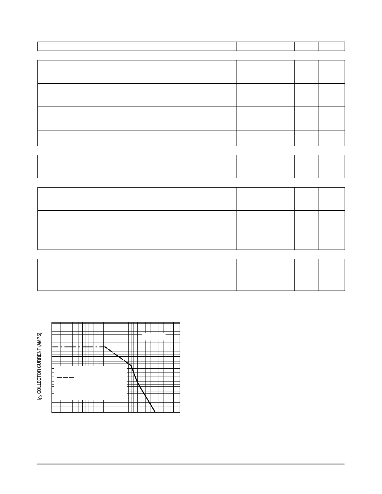
Figure 1. Active−Region Safe Operating Area
There are two limitations on the powerhandling ability of
a transistor: average junction temperature and second
breakdown. Safe operating area curves indicate IC − VCE
limits of the transistor that must be observed for reliable
operation; i.e., the transistor must not be subjected to greater
dissipation than the curves indicate.
The data of Figure 1 is based on TJ(pk) = 200_C; TC is
variable depending on conditions. At high case
temperatures, thermal limitations will reduce the power that
can be handled to values Ion than the limitations imposed by
second breakdown.
http://onsemi.com
2
Share Link: 