IRFP32N50 View Datasheet(PDF) - International Rectifier
Part Name
Description
MFG CO.
IRFP32N50 Datasheet PDF : 8 Pages
| |||
IRFP32N50K
Static @ TJ = 25°C (unless otherwise specified)
Symbol
V(BR)DSS
∆V(BR)DSS/∆TJ
RDS(on)
VGS(th)
Parameter
Drain-to-Source Breakdown Voltage
Breakdown Voltage Temp. Coefficient
Static Drain-to-Source On-Resistance
Gate Threshold Voltage
IDSS
Drain-to-Source Leakage Current
Gate-to-Source Forward Leakage
IGSS
Gate-to-Source Reverse Leakage
Min. Typ. Max. Units
Conditions
500 ––– ––– V VGS = 0V, ID = 250µA
––– 0.54 ––– V/°C Reference to 25°C, ID = 1mA
––– 0.135 0.16 Ω VGS = 10V, ID = 32A
3.0 ––– 5.0 V VDS = VGS, ID = 250µA
––– ––– 50 µA VDS = 500V, VGS = 0V
––– ––– 250 µA VDS = 400V, VGS = 0V, TJ = 150°C
––– ––– 100 nA VGS = 30V
––– ––– -100
VGS = -30V
Dynamic @ TJ = 25°C (unless otherwise specified)
Parameter
Min. Typ. Max. Units
Conditions
gfs
Forward Transconductance
14 ––– ––– S VDS = 50V, ID = 32A
Qg
Total Gate Charge
––– ––– 190
ID = 32A
Qgs
Gate-to-Source Charge
Qgd
Gate-to-Drain ("Miller") Charge
––– ––– 59
––– ––– 84
nC VDS = 400V
VGS = 10V
td(on)
Turn-On Delay Time
––– 28 –––
VDD = 250V
tr
td(off)
tf
Rise Time
Turn-Off Delay Time
Fall Time
––– 120 ––– ns ID = 32A
––– 48 –––
RG = 4.3Ω
––– 54 –––
VGS = 10V
Ciss
Input Capacitance
––– 5280 –––
VGS = 0V
Coss
Output Capacitance
––– 550 –––
VDS = 25V
Crss
Reverse Transfer Capacitance
––– 45 ––– pF ƒ = 1.0MHz, See Fig. 5
Coss
Output Capacitance
––– 5630 –––
VGS = 0V, VDS = 1.0V, ƒ = 1.0MHz
Coss
Coss eff.
Output Capacitance
Effective Output Capacitance
––– 155 –––
––– 265 –––
VGS = 0V, VDS = 400V, ƒ = 1.0MHz
VGS = 0V, VDS = 0V to 400V
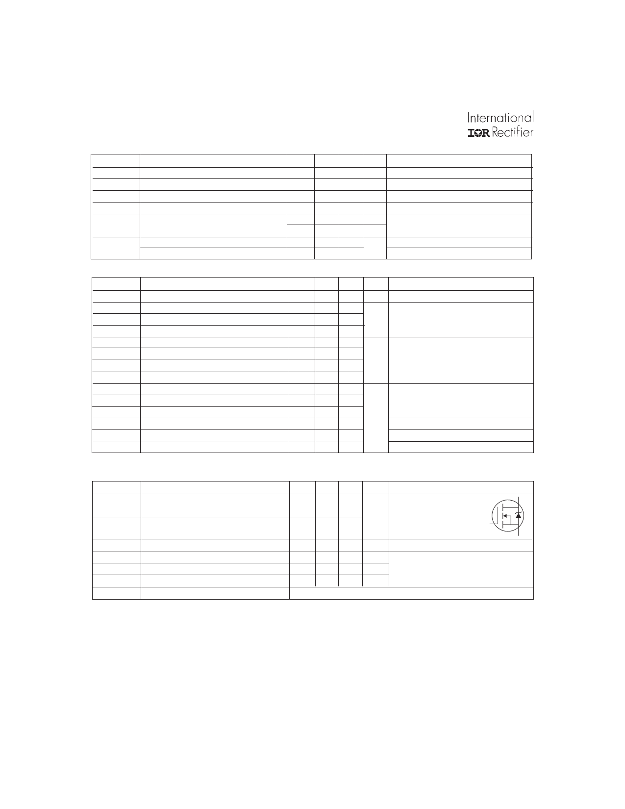
Diode Characteristics
Symbol
Parameter
IS
Continuous Source Current
(Body Diode)
ISM
Pulsed Source Current
(Body Diode)
VSD
trr
Qrr
IRRM
ton
Diode Forward Voltage
Reverse Recovery Time
Reverse RecoveryCharge
Reverse RecoveryCurrent
Forward Turn-On Time
Min. Typ. Max. Units
Conditions
MOSFET symbol
D
––– ––– 32
A showing the
integral reverse
G
––– ––– 130
p-n junction diode.
S
––– ––– 1.5 V TJ = 25°C, IS = 32A, VGS = 0V
––– 530 800 ns TJ = 25°C, IF = 32A
––– 9.0 13.5 µC di/dt = 100A/µs
––– 30 ––– A
Intrinsic turn-on time is negligible (turn-on is dominated by LS+LD)
Notes:
Repetitive rating; pulse width limited by
max. junction temperature.
Starting TJ = 25°C, L = 0.87mH, RG = 25Ω,
IAS = 32A,
ISD ≤ 32A, di/dt ≤ 296A/µs, VDD ≤ V(BR)DSS,
TJ ≤ 150°C
2
Pulse width ≤ 400µs; duty cycle ≤ 2%.
Coss eff. is a fixed capacitance that gives the same charging time
as Coss while VDS is rising from 0 to 80% VDSS.
Rθ is measured at TJ approximately 90°C
www.irf.com
Share Link: 