HEF4050B View Datasheet(PDF) - NXP Semiconductors.
Part Name
Description
MFG CO.
HEF4050B Datasheet PDF : 11 Pages
| |||
NXP Semiconductors
HEF4050B
Hex non-inverting buffers
VDD
VI
G
VO
DUT
RT
CL
001aag182
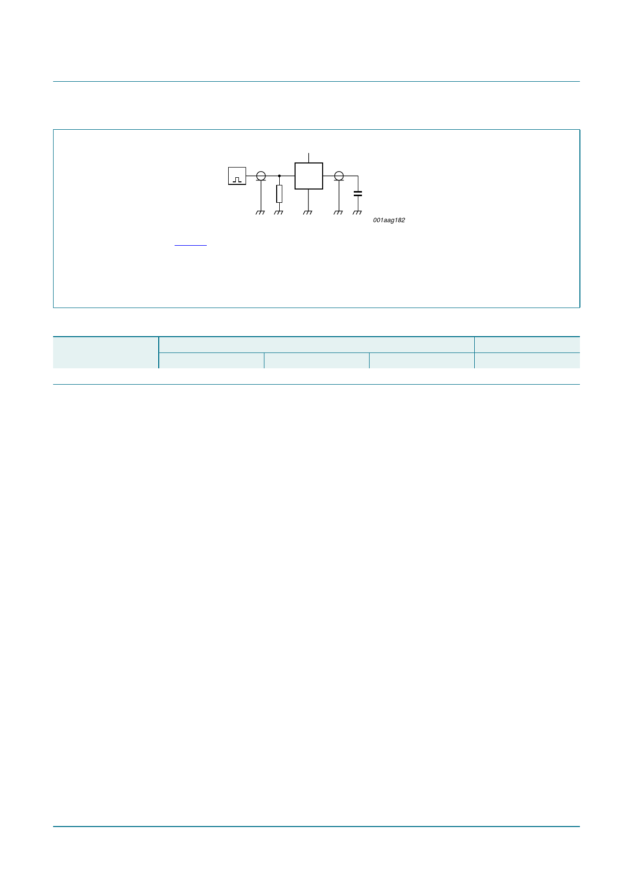
Fig 6.
Test data is given in Table 10.
Definitions for test circuit:
CL = Load capacitance including jig and probe capacitance.
RT = Termination resistance should be equal to output impedance Zo of the pulse generator.
Test circuit for switching times
Table 10. Test data
Supply voltage
5 V to 15 V
Input
VI
VDD
VM
0.5VI
tr, tf
≤ 20 ns
Load
CL
50 pF
HEF4050B_5
Product data sheet
Rev. 05 — 11 November 2008
© NXP B.V. 2008. All rights reserved.
6 of 11
Share Link: 