SAF-C504 View Datasheet(PDF) - Siemens AG
Part Name
Description
MFG CO.
SAF-C504 Datasheet PDF : 49 Pages
| |||
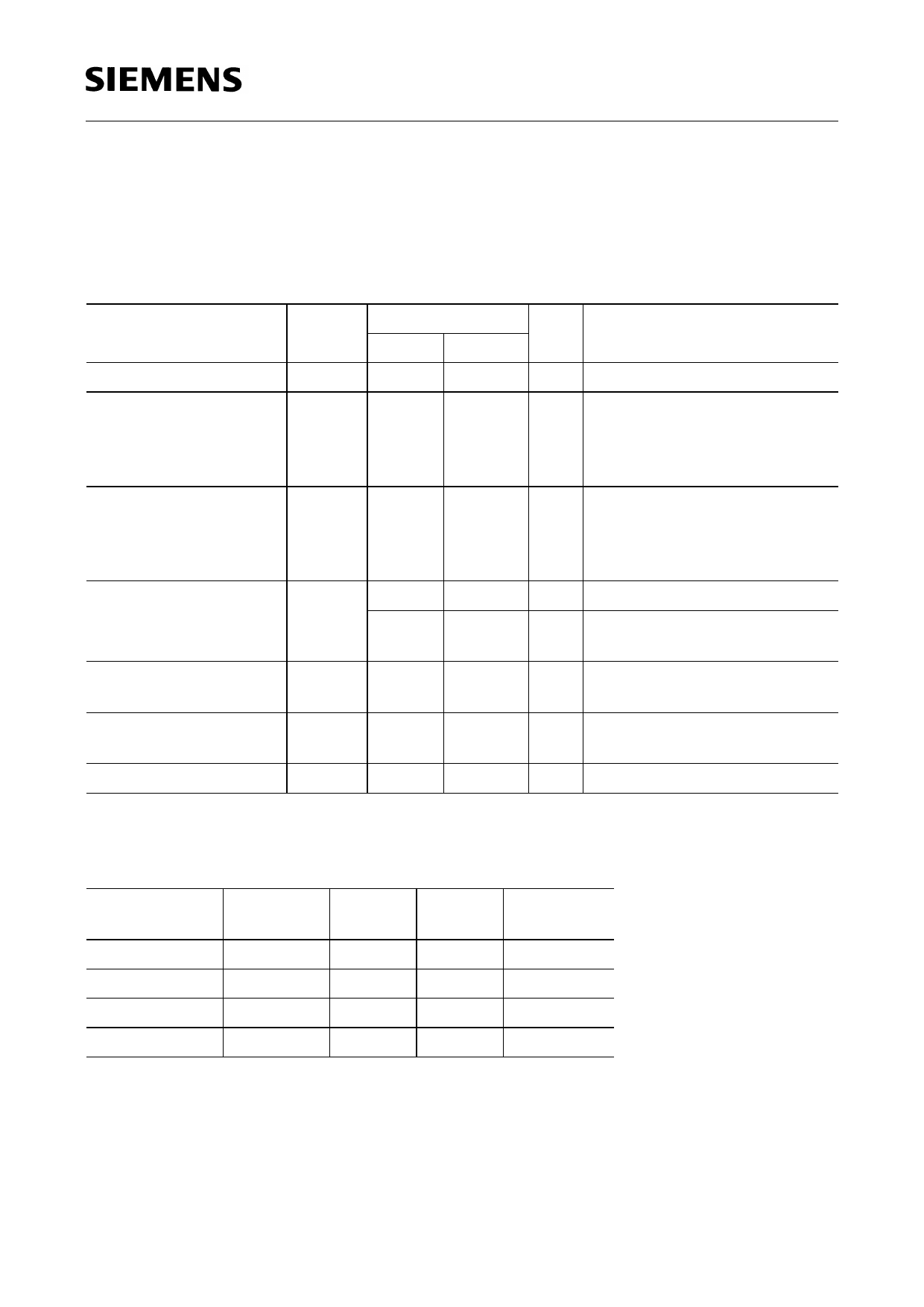
C504
A/D Converter Characteristics
VCC = 5 V + 10%, – 15%; VSS = 0 V
4V ≤ VAREF ≤ VCC + 0.1 V;
VSS – 0.1 V ≤ VAGND ≤ VSS + 0.2 V;
TA = 0 to 70 °C
TA = – 40 to 85 °C
TA = – 40 to 110 °C
TA = – 40 to 125 °C
for the SAB-C504
for the SAF-C504
for the SAH-C504
for the SAK-C504
Parameter
Analog input voltage
Sample time
Symbol
VAIN
tS
Conversion cycle time tADCC
Total unadjusted error TUE
Internal resistance of
RAREF
reference voltage source
Internal resistance of
analog source
RASRC
ADC input capacitance CAIN
Limit Values
min. max.
VAGND
–
–
–
VAREF
64 x tIN
32 x tIN
16 x tIN
8 x tIN
384 x tIN
192 x tIN
96 x tIN
48 x tIN
±2
–
±4
Unit
V
ns
ns
LSB
LSB
–
tADC / 250 kΩ
– 0.25
–
tS / 500 kΩ
– 0.25
–
50
pF
Test Condition
1)
Prescaler ÷ 32
Prescaler ÷ 16
Prescaler ÷ 8
Prescaler ÷ 4 2)
Prescaler ÷ 32
Prescaler ÷ 16
Prescaler ÷ 8
Prescaler ÷ 4 3)
VSS + 0.5V ≤ VIN ≤ VCC – 0.5V 4)
VSS < VIN < VSS + 0.5V
VCC – 0.5V < VIN < VCC
4)
tADC in [ns] 5) 6)
tS in [ns] 2) 6)
6)
Notes see next page.
Clock calculation table :
Clock Prescaler
Ratio
÷ 32
÷ 16
÷8
÷4
ADCL1, 0 tADC
11
10
01
00
32 x tIN
16 x tIN
8 x tIN
4 x tIN
tS
64 x tIN
32 x tIN
16 x tIN
8 x tIN
Further timing conditions : tADC min = 500 ns
tIN = 2 / fOSC = 2 tCLCL
tADCC
384 x tIN
192 x tIN
96 x tIN
48 x tIN
Semiconductor Group
37
Share Link: 