ADUC814BRU View Datasheet(PDF) - Analog Devices
Part Name
Description
MFG CO.
ADUC814BRU Datasheet PDF : 72 Pages
| |||
ADuC814
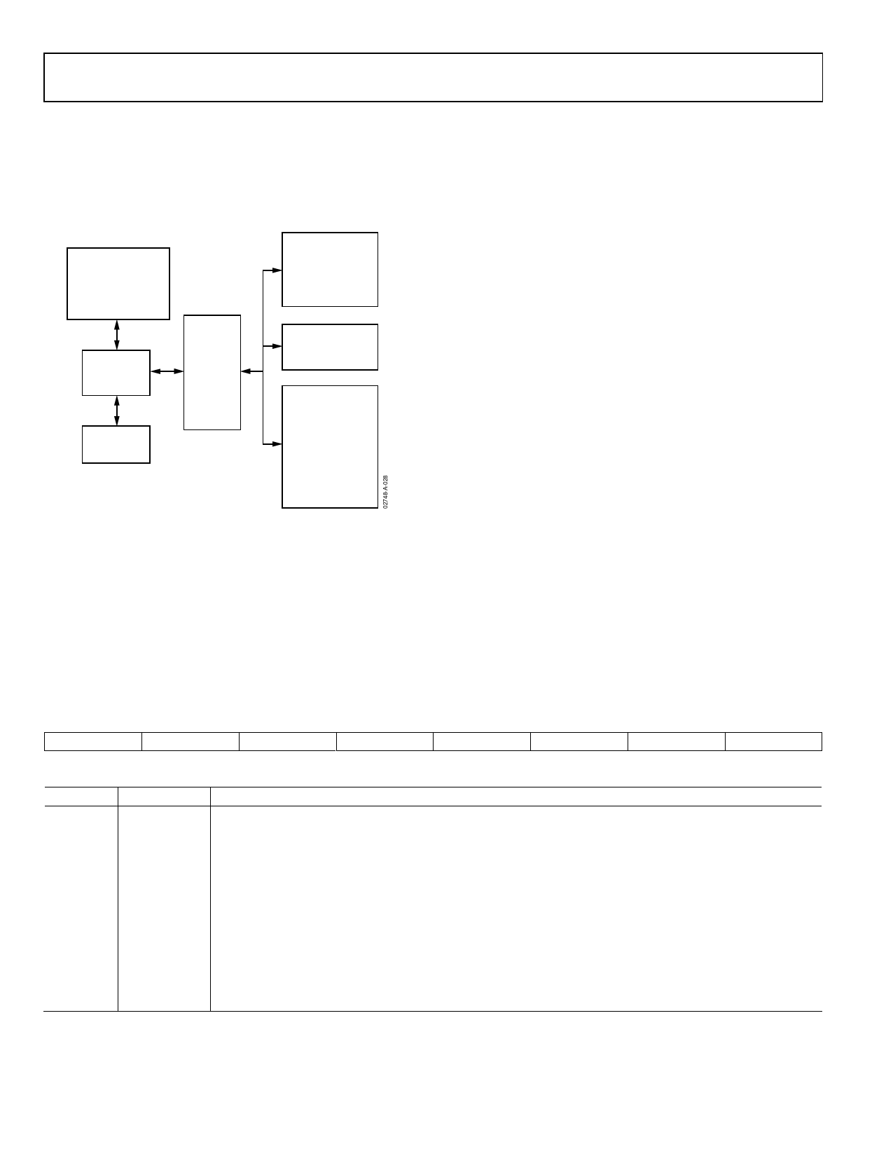
The SFR space is mapped to the upper 128 bytes of internal
data memory space and is accessed by direct addressing only. It
provides an interface between the CPU and all on-chip periph-
erals. A block diagram showing the programming model of the
ADuC814 via the SFR area is shown in Figure 21. A complete
SFR map is shown in Figure 22.
8-kBYTE
ELECTRICALLY
REPROGRAMMABLE
NONVOLATILE
FLASH/EE PROGRAM
MEMORY
640-BYTE
ELECTRICALLY
REPROGRAMMABLE
NONVOLATILE
FLASH/EE DATA
MEMORY
8051
COMPATIBLE
CORE
256 BYTES
RAM
128-BYTE
SPECIAL
FUNCTION
REGISTER
AREA
6-CHANNEL
12-BIT SAR ADC
OTHER ON-CHIP
PERIPHERALS
TEMPERATURE
MONITOR
DUAL 12-BIT DAC
SERIAL I/O
WDT
PSM
TIC
PLL
Figure 21. Programming Model
OVERVIEW OF MCU-RELATED SFRS
Accumulator SFR
ACC is the accumulator register and is used for math operations
including addition, subtraction, integer multiplication and
division, and Boolean bit manipulations. The mnemonics for
accumulator-specific instructions refer to the accumulator as A.
B SFR
The B register is used with the ACC for multiplication and
division operations. For other instructions it can be treated as a
general-purpose scratchpad register.
Stack Pointer SFR
The SP register is the stack pointer and is used to hold an internal
RAM address called the top of the stack. The SP register is
incremented before data is stored during PUSH and CALL
executions. While the stack may reside anywhere in on-chip
RAM, the SP register is initialized to 07H after a reset. This
causes the stack to begin at location 08H.
Data Pointer
The data pointer is made up of two 8-bit registers, named DPH
(high byte) and DPL (low byte). These registers provide memory
addresses for internal code access. The pointer may be manipu-
lated as a 16-bit register (DPTR = DPH, DPL), or as two inde-
pendent 8-bit registers (DPH, DPL).
Program Status Word SFR
The program status word (PSW) register is the program status word that contains several bits reflecting the current status of the CPU as
detailed in Table 4.
SFR Address
Power-On Default
Bit Addressable
D0H
00H
Yes
CY
AC
F0
RS1
RS0
OV
F1
P
Table 4. PSW SFR Bit Designations
Bit No. Name
Description
7
CY
Carry Flag.
6
AC
Auxiliary Carry Flag.
5
F0
General-Purpose Flag.
4
RS1
Register Bank Select Bits.
3
RS0
RS1 RS0 Selected Bank
0
0
0
0
1
1
1
0
2
1
1
3
2
OV
Overflow Flag.
1
F1
General-Purpose Flag.
0
P
Parity Bit.
Rev. A | Page 18 of 72
Share Link: 