CY8C4124PVQ-473 View Datasheet(PDF) - Cypress Semiconductor
Part Name
Description
MFG CO.
CY8C4124PVQ-473 Datasheet PDF : 43 Pages
| |||
PSoC® 4: PSoC 4100 Family
Datasheet
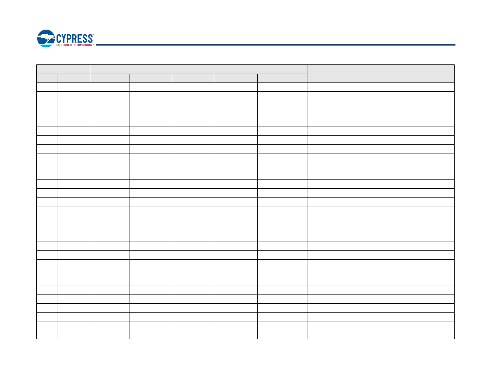
The following is the pin-list for the PSoC 4100 (35-WLCSP).
35-Ball CSP
Pin
Name
D3
P2.2
E4
P2.3
E5
P2.4
E6
P2.5
E3
P2.6
E2
P2.7
E1
P3.0
D2
P3.1
D1
P3.2
B7
VSS
C1
P3.3
C2
P3.4
B1
P4.0
B2
P4.1
A2
P4.2
A1
P4.3
C3
P0.0
A5
P0.1
A4
P0.2
A3
P0.3
B3
P0.4
A6
P0.5
B4
P0.6
B5
P0.7
B6
XRES
A7
VCCD
C7
VDD
C4
P1.0
C5
P1.1
Analog
sarmux.2
sarmux.3
sarmux.4
sarmux.5
sarmux.6
sarmux.7
–
–
–
–
–
–
–
–
csd_c_mod
csd_c_sh_tank
comp1_inp
comp1_inn
comp2_inp
comp2_inn
–
–
–
–
–
–
–
ctb.oa0.inp
ctb.oa0.inm
Alternate Functions for Pins
Alt 1
Alt 2
Alt 3
Alt 4
Pin Description
–
–
–
–
Port 2 Pin 2: gpio, lcd, csd, sarmux
–
–
–
–
Port 2 Pin 3: gpio, lcd, csd, sarmux
tcpwm0_p[1]
–
–
–
Port 2 Pin 4: gpio, lcd, csd, sarmux, pwm
tcpwm0_n[1]
–
–
–
Port 2 Pin 5: gpio, lcd, csd, sarmux, pwm
tcpwm1_p[1]
–
–
–
Port 2 Pin 6: gpio, lcd, csd, sarmux, pwm
tcpwm1_n[1]
–
–
–
Port 2 Pin 7: gpio, lcd, csd, sarmux, pwm
tcpwm0_p[0] scb1_uart_rx[0] scb1_i2c_scl[0] scb1_spi_mosi[0] Port 3 Pin 0: gpio, lcd, csd, pwm, scb1
tcpwm0_n[0] scb1_uart_tx[0] scb1_i2c_sda[0] scb1_spi_miso[0] Port 3 Pin 1: gpio, lcd, csd, pwm, scb1
tcpwm1_p[0]
–
swd_io[0]
scb1_spi_clk[0] Port 3 Pin 2: gpio, lcd, csd, pwm, scb1, swd
–
–
–
–
Ground
tcpwm1_n[0]
–
swd_clk[0] scb1_spi_ssel_0[0] Port 3 Pin 3: gpio, lcd, csd, pwm, scb1, swd
tcpwm2_p[0]
-
–
scb1_spi_ssel_1 Port 3 Pin 4: gpio, lcd, csd, pwm, scb1
–
scb0_uart_rx scb0_i2c_scl scb0_spi_mosi Port 4 Pin 0: gpio, lcd, csd, scb0
–
scb0_uart_tx scb0_i2c_sda scb0_spi_miso Port 4 Pin 1: gpio, lcd, csd, scb0
–
–
–
scb0_spi_clk Port 4 Pin 2: gpio, lcd, csd, scb0
–
–
–
scb0_spi_ssel_0 Port 4 Pin 3: gpio, lcd, csd, scb0
–
–
–
scb0_spi_ssel_1 Port 0 Pin 0: gpio, lcd, csd, scb0, comp
–
–
–
scb0_spi_ssel_2 Port 0 Pin 1: gpio, lcd, csd, scb0, comp
–
–
–
scb0_spi_ssel_3 Port 0 Pin 2: gpio, lcd, csd, scb0, comp
–
–
–
–
Port 0 Pin 3: gpio, lcd, csd, comp
–
scb1_uart_rx[1] scb1_i2c_scl[1] scb1_spi_mosi[1] Port 0 Pin 4: gpio, lcd, csd, scb1
–
scb1_uart_tx[1] scb1_i2c_sda[1] scb1_spi_miso[1] Port 0 Pin 5: gpio, lcd, csd, scb1
ext_clk
–
–
scb1_spi_clk[1] Port 0 Pin 6: gpio, lcd, csd, scb1, ext_clk
–
–
wakeup
scb1_spi_ssel_0[1] Port 0 Pin 7: gpio, lcd, csd, scb1, wakeup
–
–
–
–
Chip reset, active low
–
–
–
–
Regulated supply, connect to 1µF cap or 1.8V
–
–
–
–
Supply, 1.8 - 5.5V
tcpwm2_p[1]
–
–
–
Port 1 Pin 0: gpio, lcd, csd, ctb, pwm
tcpwm2_n[1]
–
–
–
Port 1 Pin 1: gpio, lcd, csd, ctb, pwm
Document Number: 001-87220 Rev. *J
Page 11 of 43
Share Link: 