VO14642AABTR View Datasheet(PDF) - Vishay Semiconductors
Part Name
Description
MFG CO.
VO14642AABTR Datasheet PDF : 10 Pages
| |||
www.vishay.com
VO14642AT, VO14642AABTR
Vishay Semiconductors
ABSOLUTE MAXIMUM RATINGS (Tamb = 25 °C, unless otherwise specified)
PARAMETER
TEST CONDITION
SYMBOL
VALUE
UNIT
INPUT
LED continous forward current
IF
50
mA
LED reverse voltage
VR
5
V
LED power dissipation
OUTPUT
At 25 °C
Pdiss
80
mW
DC or peak AC load voltage
VL
60
V
Load current (DC only)
IL
2
A
Peak load current (AC/DC)
t = 10 ms
ILPK
3.6
A
Output power dissipation
At 25 °C
Pdiss
250
mW
SSR
Total power dissipation
Pdiss
330
mW
Ambient temperature range
Tamb
-55 to +85
°C
Storage temperature range
Soldering temperature (1)
Tstg
-55 to +125
°C
t ≤ 10 s max.
Tsld
260
°C
Notes
• Stresses in excess of the absolute maximum ratings can cause permanent damage to the device. Functional operation of the device is not
implied at these or any other conditions in excess of those given in the operational sections of this document. Exposure to absolute
maximum ratings for extended periods of the time can adversely affect reliability
(1) Refer to reflow profile for soldering conditions for surface mounted devices (SMD). Refer to wave profile for soldering conditions for through
hole devices (DIP)
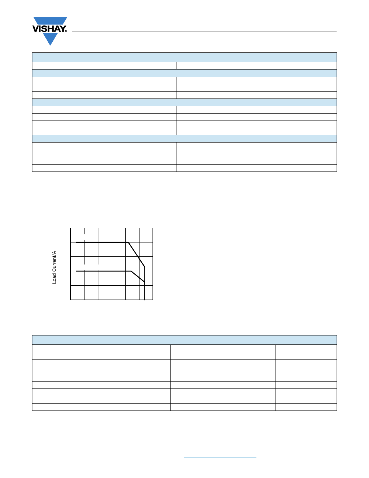
ABSOLUTE MAXIMUM RATING CURVE
2.5
DC mode
2.0
1.5
AC/DC mode
1.0
0.5
0.0
-50 -25 0 25 50 75 100
Ambient Temperature/°C
Fig. 1 - Load Current (AC/DC) vs. Temperature
THERMAL CHARACTERISTICS
PARAMETER
TEST CONDITION
SYMBOL VALUE
UNIT
Maximum LED junction temperature
Maximum output die junction temperature
Thermal resistance, junction emitter to board
Thermal resistance, junction emitter to case
Thermal resistance, junction detector to board
Thermal resistance, junction detector to case
Thermal resistance, junction emitter to junction detector
Thermal resistance, case to ambient
At 25 °C
At 25 °C
At 25 °C
At 25 °C
At 25 °C
At 25 °C
At 25 °C
At 25 °C
Tjmax.
Tjmax.
θEB
θEC
θDB
θDC
θED
θCA
125
125
176
208
67
134
310
2180
°C
°C
°C/W
°C/W
°C/W
°C/W
°C/W
°C/W
Note
• The thermal model is represented in the thermal network below. Each resistance value given in this model can be used to calculate the
temperatures at each node for a given operating condition. The thermal resistance from board to ambient will be dependent on the type of
PCB, layout and thickness of copper traces. For a detailed explanation of the thermal model, please reference Vishay's thermal
characteristics of optocouplers application note
Rev. 1.6, 12-Jun-17
2
Document Number: 81646
For technical questions, contact: optocoupleranswers@vishay.com
THIS DOCUMENT IS SUBJECT TO CHANGE WITHOUT NOTICE. THE PRODUCTS DESCRIBED HEREIN AND THIS DOCUMENT
ARE SUBJECT TO SPECIFIC DISCLAIMERS, SET FORTH AT www.vishay.com/doc?91000
Share Link: 