UPD6345C View Datasheet(PDF) - NEC => Renesas Technology
Part Name
Description
MFG CO.
UPD6345C Datasheet PDF : 16 Pages
| |||
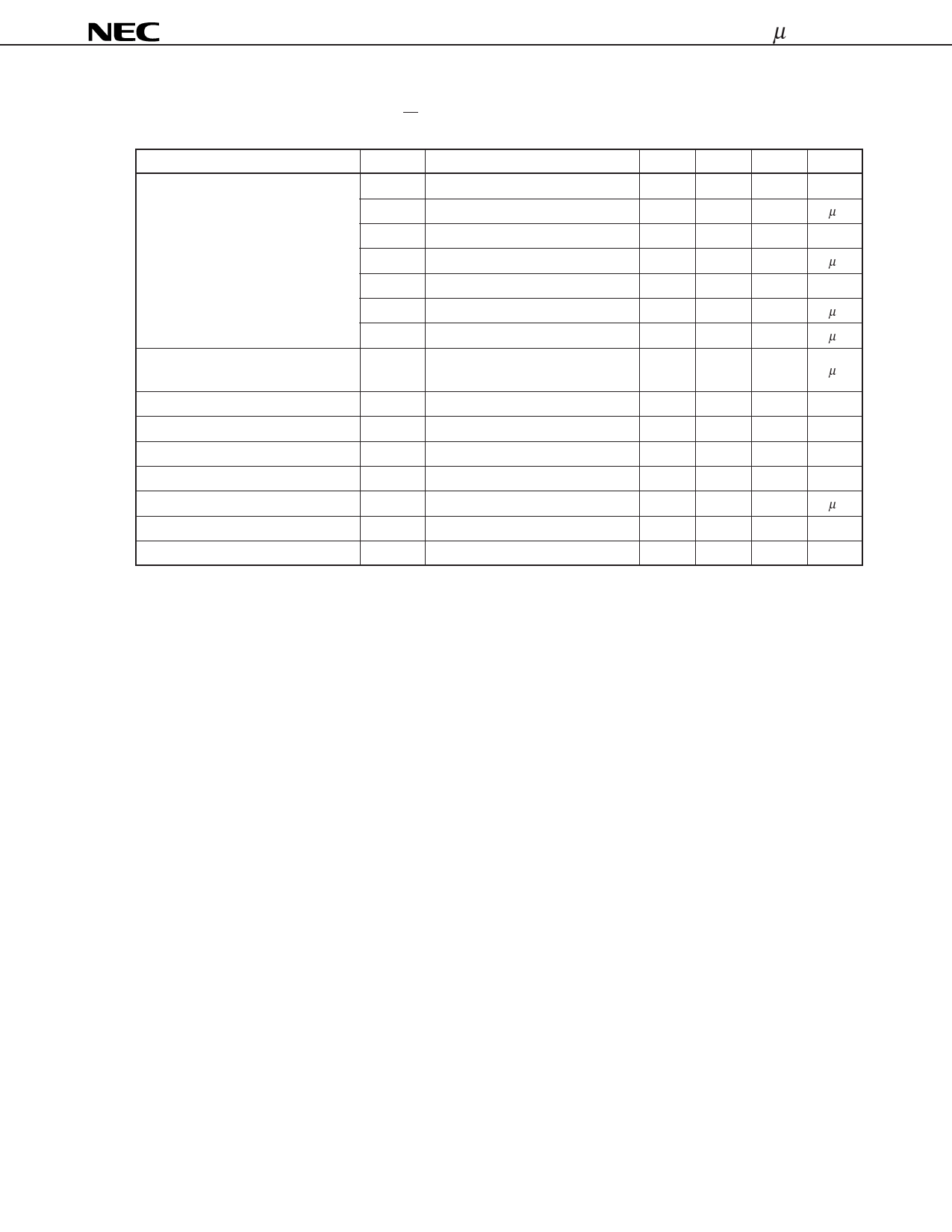
µPD6345
SWITCHING CHARACTERISTICS
(Ta = 25 °C, VDD = 5 V, CL = 15 pF, R (On) = 300 Ω, VOUT = 12 V, tr = tf = 6 ns)
ITEM
SYMBOL
CONDITION
tPLH1
SCK → SO (High Level)
tPLH2
SCK → Driver Output (High Level)
tPHL1
SCK → SO (Low Level)
Propagation Delay Time
tPHL2
SCK →Driver Output (Low Level)
tPHL3
RESET → SO
tPHL/PLH4 Output Enable → Driver Output
tPHL/PLH5 Latch Enable → Driver Output
Clock Transition Time
tr
SCK
tf
Maximum Clock Frequency
fmax
Minimum Data Setup Time
tSETUP
Minimum Data Hold Time
tHOLD
Minimum Reset Pulse Width
PWRESET
Minimum Output Enable Pulse Width PWENABLE
Minimum Latch Enable Pulse Width PWLATCH
Clock Pulse Width
PWSCK
MIN.
20
20
20
20
62.5
1
62.5
TYP.
70
13
10
10
10
0.55
38
38
MAX.
100
1
100
1
100
1
1
UNIT
ns
µs
ns
µs
ns
µs
µs
µs
8
62.5
MHz
ns
ns
ns
µs
ns
ns
7
Share Link: 