TC74AC377 View Datasheet(PDF) - Toshiba
Part Name
Description
MFG CO.
TC74AC377 Datasheet PDF : 3 Pages
| |||
TC74AC377
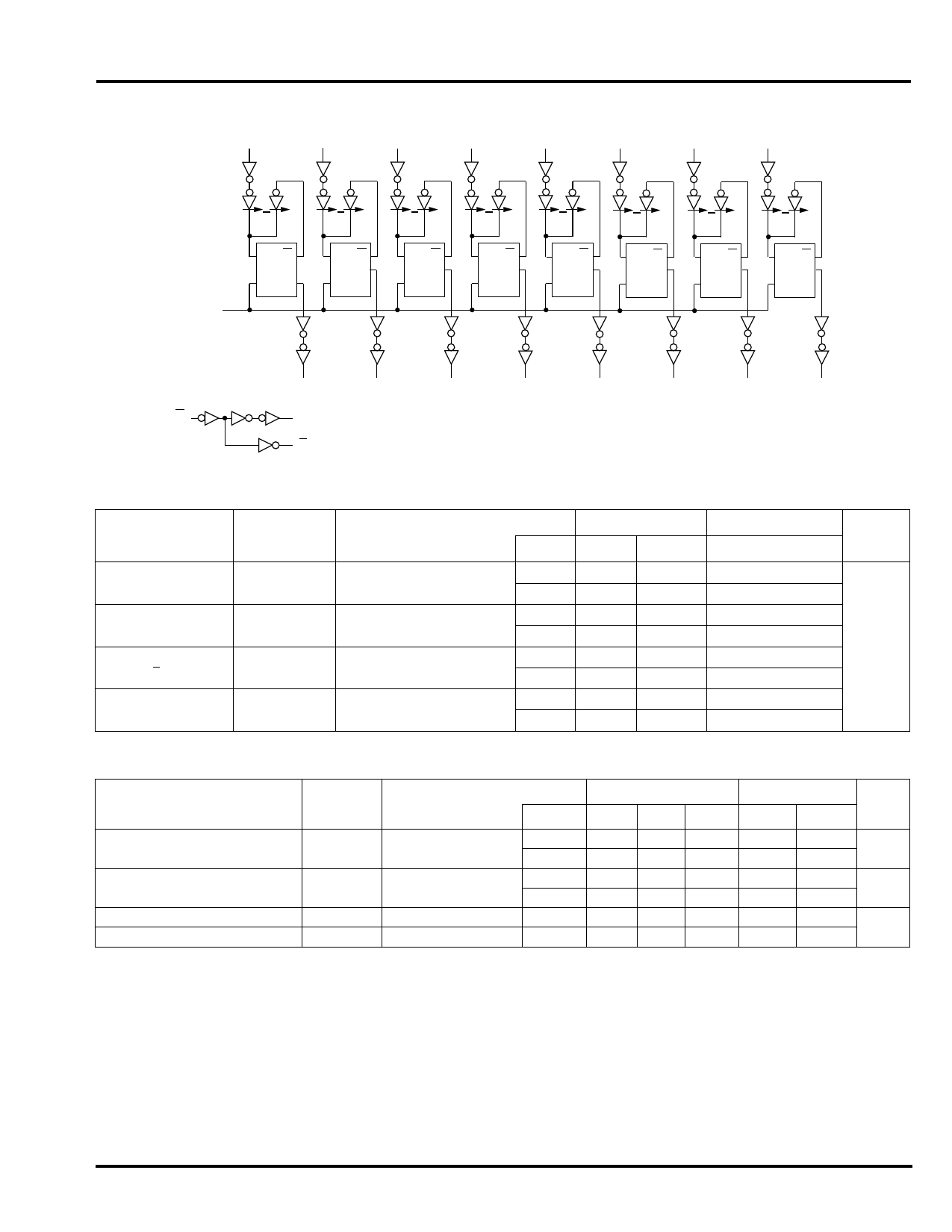
System Diagram
D1
D2
D3
D4
D5
D6
D7
D8
3
4
7
8
13
14
17
18
EE
EE
EE
EE
EE
EE
EE
EE
11
CLOCK
DQ
CK Q
DQ
CK Q
DQ
CK Q
DQ
CK Q
DQ
CK Q
DQ
CK Q
DQ
CK Q
DQ
CK Q
2
5
6
9
12
15
16
19
Q1
Q2
Q3
Q4
Q5
Q6
Q7
Q8
G1
E
E
Timing Requirements (Input tr = tf = 3n)
PARAMETER
SYMBOL
TEST CONDITION
Minimum Pulse Width (CK)
tW(L)
—
tW(H)
Minimum Set-up Time
(D–CK)
tW(L)
—
Minimum Set-up Time
(G–CK)
ts
—
Minimum Hold Time
th
—
VCC
3.3±0.3
5.0±0.5
3.3±0.3
5.0±0.5
3.3±0.3
5.0±0.5
3.3±0.3
5.0±0.5
Ta=25˚C
Typ.
Max.
—
8.0
—
5.0
—
8.0
—
4.0
—
9.0
—
4.0
—
1.0
—
1.0
Ta= –40~85˚
Max.
8.0
5.0
8.0
4.0
9.0
4.0
1.0
1.0
UNIT
ns
AC Electrical Characteristics (CL = 50pF, RL = 500Ω, Input tr = tf = 3ns)
PARAMETER
Propagation Delay Time
(CK–Q)
Maximum Clock Frequency
Input Capacitance
Power Dissipation Capacitance
SYMBOL
tpLH
tpHL
fMAX
CIN
CPD1
TEST CONDITION
—
—
—
—
VCC
3.0±0.3
5.0±0.5
3.0±0.3
5.0±0.5
—
—
Ta = 25°C
Min. Typ. Max.
—
10.6
17.6
—
7.4
10.6
50
95
—
80
140
—
—
5
10
—
30
—
Ta = -40~85°C
Min.
Max.
1.0
20.0
1.0
12.0
50
—
80
—
—
10
—
—
UNIT
ns
MHz
pF
Note (1): CPD is defined as the value of the internal equivalent capacitance which is calculated from the operating current consumption without load.
Average operating current can be obtained by the equation: ICC (opr) = CPD • VCC • fIN + ICC / 8 (per F/F).
And the total CPD when n pcs. of Flip-Flop operate can be gained by the following equation: CPD (total)=20+10 • n.
TOSHIBA CORPORATION
3/3
Share Link: 