NB100LVEP91(2003) View Datasheet(PDF) - ON Semiconductor
Part Name
Description
MFG CO.
NB100LVEP91
(Rev.:2003)
(Rev.:2003)
ON Semiconductor
NB100LVEP91 Datasheet PDF : 8 Pages
| |||
NB100LVEP91
MAXIMUM RATINGS (Note 2)
Symbol
Parameter
Condition 1
Condition 2 Rating
Unit
VCC
PECL Power Supply
VEE
NECL Power Supply
VI
PECL Input Voltage
VOP
Operating Voltage
Iout
Output Current
GND = 0 V
GND = 0 V
GND = 0 V
GND = 0 V
Continuous
Surge
3.8 to 0
V
-5.5 to 0
V
VI VCC
3.8 to 0
V
VCC - VEE
9.3 to 0
V
50
mA
100
mA
IBB
PECL VBB Sink/Source
TA
Operating Temperature Range
Tstg
Storage Temperature Range
qJA
Thermal Resistance (Junction-to-Ambient)
JESD 51-3 (1S-Single Layer Test Board)
0 lFPM
500 LFPM
qJA
Thermal Resistance (Junction-to-Ambient)
0 LFPM
JESD 51- 6 (2S2P Multilayer Test Board) with Filled Thermal Vias
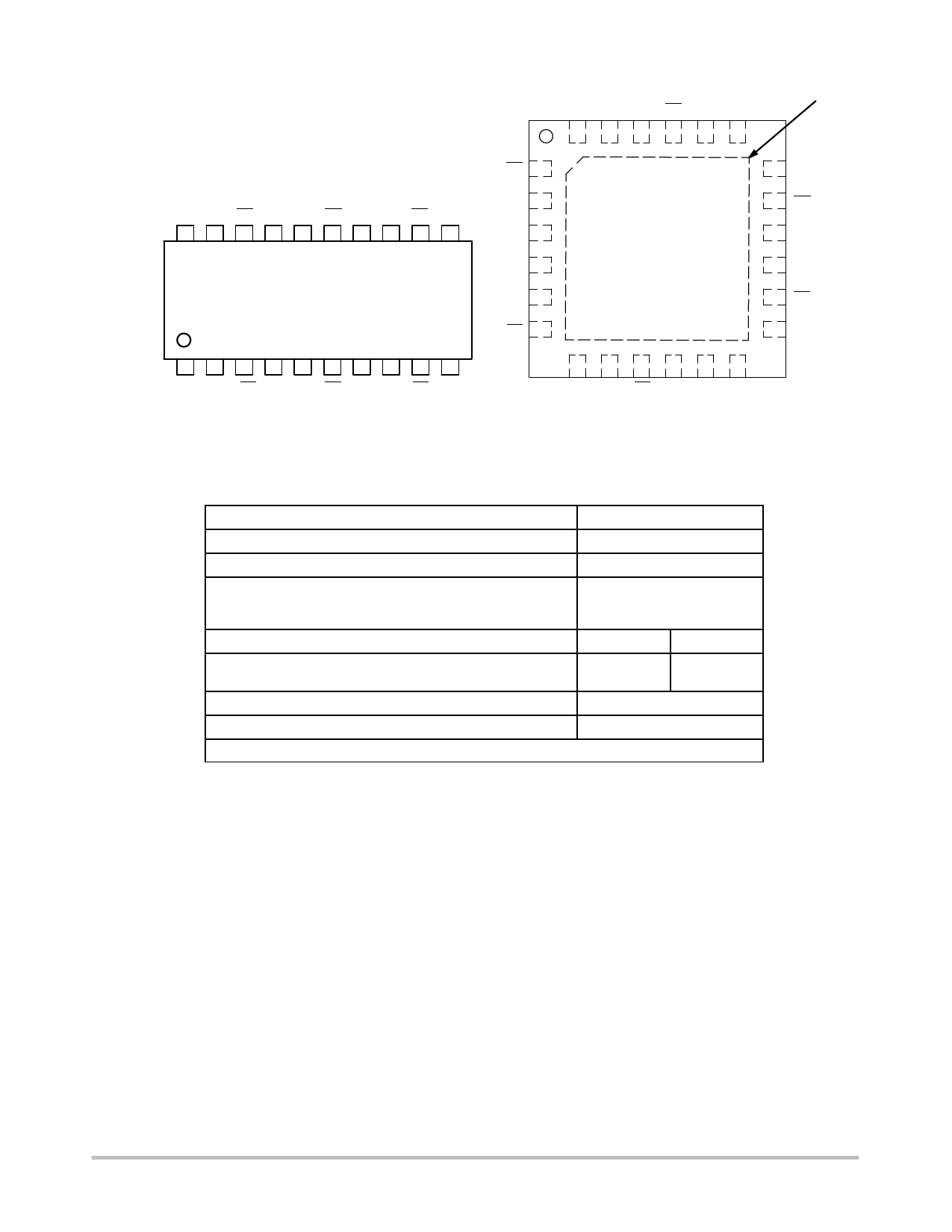
20 SOIC
20 SOIC
24 QFN
± 0.5
-40 to +85
-65 to +150
90
60
47.3
mA
°C
°C
°C/W
°C/W
°C/W
qJC
Thermal Resistance (Junction-to-Case)
std bd
Tsol
Wave Solder
<2 to 3 sec @ 248°C
2. Maximum Ratings are those values beyond which device damage may occur.
20 SOIC
30 to 35
265
°C/W
°C
LVPECL INPUT DC CHARACTERISTICS VCC = 2.5 V, VEE = -2.375 to -5.5 V, GND = 0 V (Note 3)
-40 °C
25°C
85°C
Symbol
Characteristic
Min Typ Max Min Typ Max Min Typ Max Unit
ICC
Power Supply Current
10 14 20 10 14 20 10 14 20 mA
VIH
Input HIGH Voltage
1335
VCC 1335
VCC 1275
VCC mV
VIL
VIHCMR
Input LOW Voltage
Input HIGH Voltage Common Mode Range
(Differential) (Note 4)
GND
0
875 GND
2.5
0
875 GND
2.5
0
875 mV
2.5 V
IIH
Input HIGH Current
IIL
Input LOW Current
D 0.5
D -150
150
0.5
-150
150
0.5
-150
150 mA
mA
NOTE: Devices are designed to meet the DC specifications shown in the above table, after thermal equilibrium has been established. The
circuit is in a test socket or mounted on a printed circuit board and transverse air flow greater than 500 lfpm is maintained.
3. Input parameters vary 1:1 with VCC. VCC can vary +1.3 V / -0.125 V.
4. VIHCMR min varies 1:1 with GND. VIHCMR max varies 1:1 with VCC.
LVPECL INPUT DC CHARACTERISTICS VCC = 3.3 V; VEE = -2.375 V to -5.5 V; GND = 0 V (Note 5)
-40 °C
25°C
85°C
Symbol
Characteristic
Min Typ Max Min Typ Max Min Typ Max Unit
ICC
VCC Power Supply Current
10
16 24
10
16 24
10
16 24 mA
VIH
Input HIGH Voltage (Single-Ended)
2135
VCC 2135
VCC 2135
VCC mV
VIL
Input LOW Voltage (Single-Ended)
GND
1675 GND
1675 GND
1675 mV
VBB
VIHCMR
Output Voltage Reference (Note 6)
Input HIGH Voltage Common Mode Range
(Differential) (Note 6)
1775 1875 1975 1775 1875 1975 1775 1875 1975 mV
0
3.3
0
3.3
0
3.3 V
IIH
Input HIGH Current
IIL
Input LOW Current
D 0.5
D -150
150
0.5
-150
150
0.5
-150
150 mA
mA
NOTE: Devices are designed to meet the DC specifications shown in the above table, after thermal equilibrium has been established. The
circuit is in a test socket or mounted on a printed circuit board and transverse air flow greater than 500 lfpm is maintained.
5. Input parameters vary 1:1 with VCC. VCC can vary +0.5 / -0.925 V.
6. VIHCMR min varies 1:1 with GND. VIHCMR max varies 1:1 with VCC.
http://onsemi.com
3
Share Link: 