MT88L89 View Datasheet(PDF) - Mitel Networks
Part Name
Description
MFG CO.
MT88L89 Datasheet PDF : 20 Pages
| |||
MT88L89
ACTIVE
INPUT
OUTPUT FREQUENCY (Hz)
SPECIFIED
ACTUAL
%ERROR
L1
697
699.1
+0.30
L2
770
766.2
-0.49
L3
852
847.4
-0.54
L4
941
948.0
+0.74
H1
1209
1215.9
+0.57
H2
1336
1331.7
-0.32
H3
1477
1471.9
-0.35
H4
1633
1645.0
+0.73
Table 2. Actual Frequencies Versus Standard
Requirements
Distortion Calculations
The MT88L89 is capable of producing precise tone
bursts with minimal error in frequency (see Table 2).
The internal summing amplifier is followed by a first-
order lowpass switched capacitor filter to minimize
harmonic components and intermodulation products.
The total harmonic distortion for a single tone can be
calculated using Equation 1, which is the ratio of the
total power of all the extraneous frequencies to the
power of the fundamental frequency expressed as a
percentage.
V22f + V23f + V24f + .... V2nf
THD (%) = 100
Vfundamental
Equation 1. THD (%) For a Single Tone
The Fourier components of the tone output
correspond to V2f.... Vnf as measured on the output
waveform. The total harmonic distortion for a dual
tone can be calculated using Equation 2. VL and VH
correspond to the low group amplitude and high
group amplitude, respectively and V2IMD is the sum
of all the intermodulation components. The internal
switched-capacitor filter following the D/A converter
keeps distortion products down to a very low level as
shown in Figure 10.
V22L + V23L + .... V2nL + V22H +
V23H + .. V2nH + V2IMD
THD (%) = 100
V2L + V2H
Equation 2. THD (%) For a Dual Tone
4-132
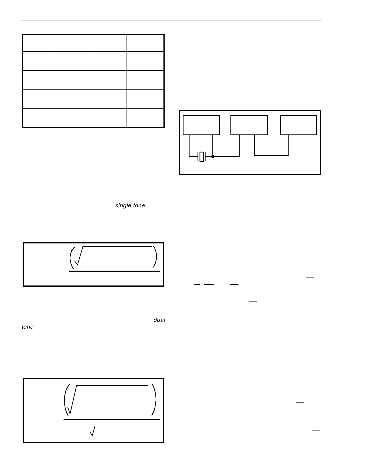
DTMF Clock Circuit
The internal clock circuit is completed with the
addition of a standard television colour burst crystal
having a resonant frequency of 3.579545 MHz. A
number of MT88L89 devices can be connected as
shown in Figure 11 such that only one crystal is
required. Alternatively, the OSC1 inputs on all
devices can be driven from a TTL buffer with the
OSC2 outputs left unconnected.
MT88L89
OSC1 OSC2
MT88L89
OSC1 OSC2
MT88L89
OSC1 OSC2
3.579545 MHz
Figure 11 - Common Crystal Connection
Microprocessor Interface
The MT88L89 design incorporates an adaptive
interface, which allows it to be connected to various
kinds of microprocessors. Key functions of this
interface include the following:
• Continuous activity on DS/RD is not necessary
to update the internal status registers.
• senses whether input timing is that of an Intel or
Motorola controller by monitoring the DS (RD),
R/W (WR) and CS inputs.
• generates equivalent CS signal for internal
operation for all processors.
• differentiates between multiplexed and non-
multiplexed microprocessor buses. Address
and data are latched in accordingly.
• compatible with Motorola and Intel processors.
Figure 16 shows the timing diagram for Motorola
microprocessors with separate address and data
buses. Members of this microprocessor family
include 2 MHz versions of the MC6800, MC6802 and
MC6809. For the MC6809, the chip select (CS) input
signal is formed by NANDing the (E+Q) clocks and
address decode output. For the MC6800 and
MC6802, CS is formed by NANDing VMA and
address decode output. On the falling edge of CS,
the internal logic senses the state of data strobe
Share Link: 