MSM56V16160D View Datasheet(PDF) - Oki Electric Industry
Part Name
Description
MFG CO.
MSM56V16160D Datasheet PDF : 30 Pages
| |||
¡ Semiconductor
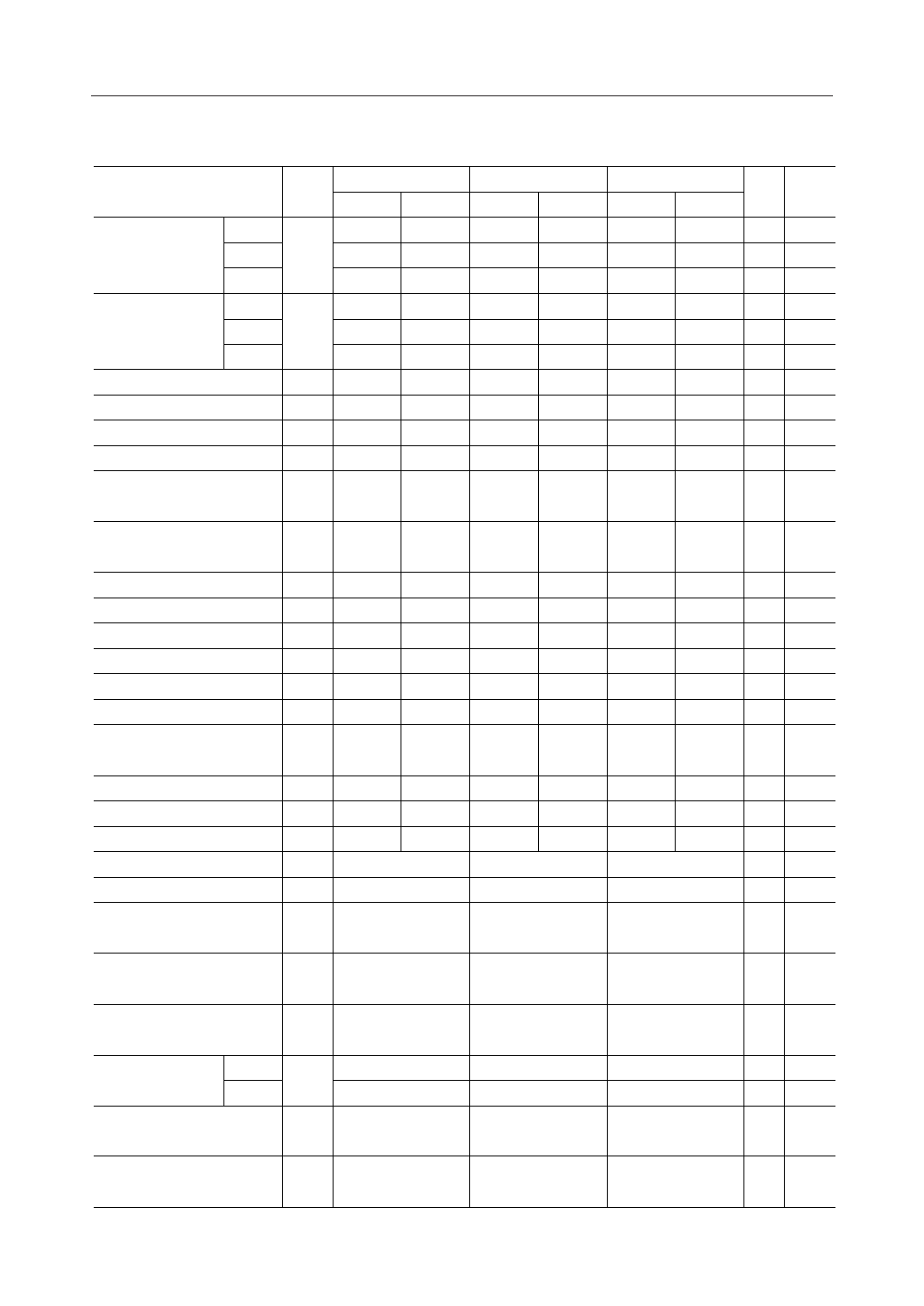
MSM56V16160D/DH
AC Characteristics
Note 1, 2
Parameter
MSM56V16160D-10 MSM56V16160D-12 MSM56V16160DH-15
Symbol
Unit Note
Min. Max. Min. Max. Min. Max.
CL = 3
10
—
12
—
15
— ns
Clock Cycles Time CL = 2 tCC
15
—
17.5
—
15
— ns
CL = 1
30
—
35
—
—
— ns
CL = 3
—
9
—
10
—
9
ns 3, 4
Access Time from CL = 2 tAC
—
9
—
14
—
9
ns 3, 4
Clock
CL = 1
—
27
—
30
—
— ns 3, 4
Clock "H" Pulse Time
Clock "L" Pulse Time
Input Setup Time
Input Hold Time
tCH
3
—
3
—
3
— ns
tCL
3
—
3
—
3
— ns
tSI
3
—
3
—
3
— ns
tHI
1
—
1
—
1
— ns
Output Low Impedance
Time from Clock
tOLZ
3
—
3
—
3
— ns
Output High Impedance
Time from Clock
tOHZ
—
8
—
10
—
8
ns
Output Hold from Clock
tOH
3
—
3
—
3
— ns 3
RAS Cycle Time
tRC
100
—
115
—
105
— ns
RAS Precharge Time
RAS Active Time
tRP
30
—
35
—
30
— ns
tRAS
60
105
70
105
70
105 ns
RAS to CAS Delay Time
tRCD
30
—
35
—
30
— ns
Write Recovery Time
tWR
15
—
24
—
15
— ns
RAS to RAS Bank Active
Delay Time
tRRD
20
—
24
—
24
— ns
Refresh Time
tREF
—
64
Power-down Exit Set-up Time tPDE tSI + 1 CLK —
Input Level Transition Time tT
CAS to CAS Delay Time (Min.) lCCD
—
3
1
Clock Disable Time from CKE lCKE
1
Data Output High Impedance
Time from UDQM, LDQM
lDOZ
2
—
64
tSI + 1 CLK —
—
3
1
1
2
—
64
tSI + 1 CLK —
—
3
1
1
2
ms
ns
ns
Cycle
Cycle
Cycle
Data Input Mask Time from
UDQM, LDQM
lDOD
0
0
0
Cycle
Data Input Time from Write
Command
lDWD
0
Data Output High
CL = 1
1
Impedance Time from
Precharge Command
CL > 1 lROH
2
Active Command Input Time from Mode
Register Set Command Input (Min.)
lMRD
3
0
0
Cycle
1
—
Cycle
2
2
Cycle
3
3
Cycle
Write Command Input Time
from Output
lOWD
2
2
2
Cycle
8/30
Share Link: 