MCM6206BAEJ15R View Datasheet(PDF) - Motorola => Freescale
Part Name
Description
MFG CO.
MCM6206BAEJ15R Datasheet PDF : 8 Pages
| |||
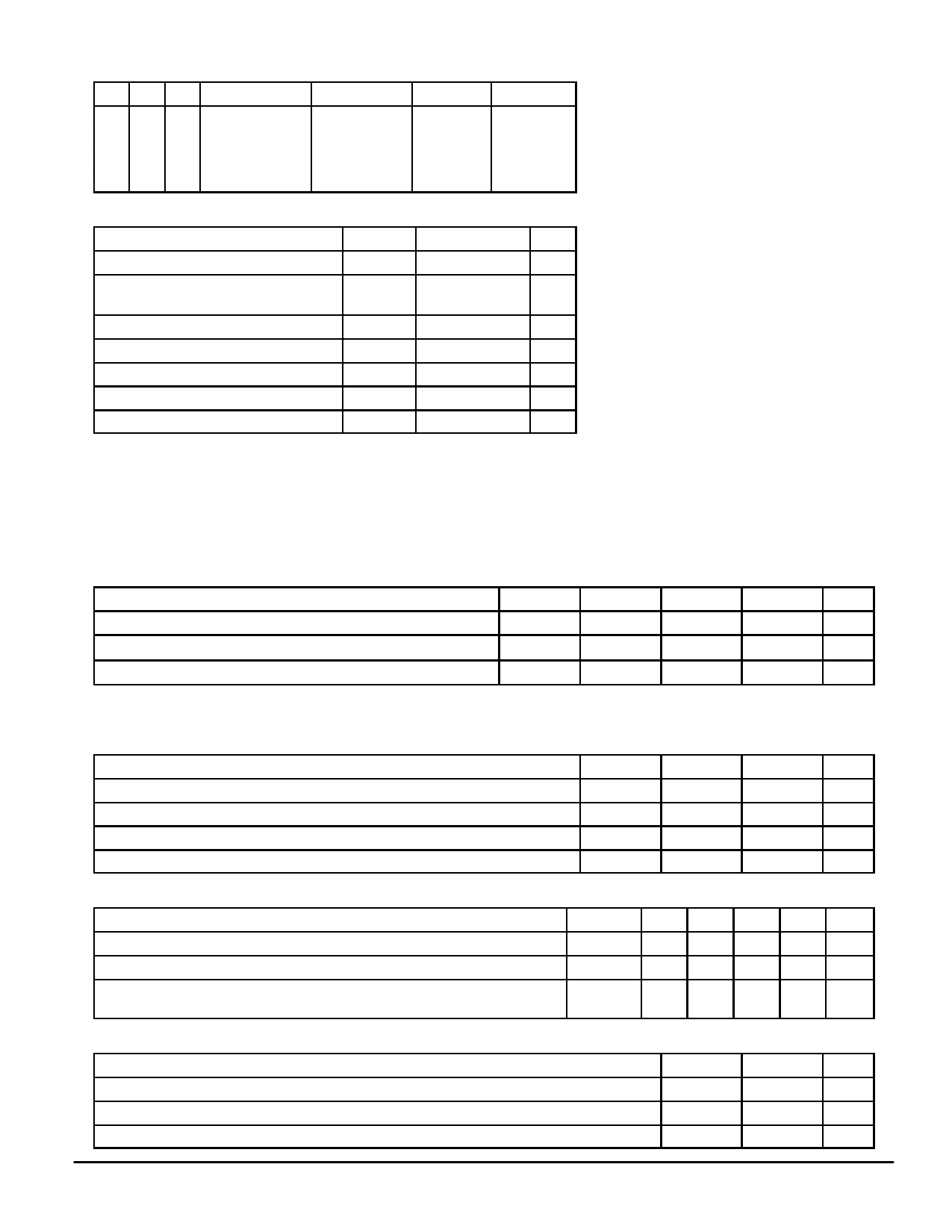
TRUTH TABLE (X = Don’t Care)
E GW
Mode
HXX
Not Selected
L H H Output Disabled
LLH
Read
LXL
Write
VCC Current
ISB1, ISB2
ICCA
ICCA
ICCA
Output
High–Z
High–Z
Dout
High–Z
Cycle
–
–
Read Cycle
Write Cycle
ABSOLUTE MAXIMUM RATINGS
Rating
Symbol
Value
Unit
Power Supply Voltage
Voltage Relative to VSS For Any Pin
Except VCC
VCC
– 0.5 to + 7.0
V
Vin, Vout – 0.5 to VCC + 0.5 V
Output Current
Iout
± 20
mA
Power Dissipation
PD
1.0
W
Temperature Under Bias
Tbias
– 10 to + 85
°C
Operating Temperature
TA
0 to + 70
°C
Storage Temperature—Plastic
Tstg
– 55 to + 125
°C
NOTE: Permanent device damage may occur if ABSOLUTE MAXIMUM RATINGS are
exceeded. Functional operation should be restricted to RECOMMENDED OPER-
ATING CONDITIONS. Exposure to higher than recommended voltages for ex-
tended periods of time could affect device reliability.
This device contains circuitry to protect the
inputs against damage due to high static volt-
ages or electric fields; however, it is advised
that normal precautions be taken to avoid
application of any voltage higher than maxi-
mum rated voltages to this high–impedance
circuit.
This CMOS memory circuit has been de-
signed to meet the dc and ac specifications
shown in the tables, after thermal equilibrium
has been established. The circuit is in a test
socket or mounted on a printed circuit board
and transverse air flow of at least 500 linear
feet per minute is maintained.
DC OPERATING CONDITIONS AND CHARACTERISTICS
(VCC = 5.0 V ±10%, TA = 0 to 70°C, Unless Otherwise Noted)
RECOMMENDED OPERATING CONDITIONS
Parameter
Symbol
Supply Voltage (Operating Voltage Range)
Input High Voltage
VCC
VIH
Input Low Voltage
VIL
* VIL (min) = – 0.5 V dc; VIL (min) = – 2.0 V ac (pulse width ≤ 20 ns)
** VIH (max) = VCC + 0.3 V dc; VIH (max) = VCC + 2.0 V ac (pulse width ≤ 20 ns)
DC CHARACTERISTICS
Parameter
Input Leakage Current (All Inputs, Vin = 0 to VCC)
Output Leakage Current (E = VIH or G = VIH, Vout = 0 to VCC)
Output High Voltage (IOH = – 4.0 mA)
Output Low Voltage (IOL = 8.0 mA)
Min
4.5
2.2
– 0.5*
Symbol
Ilkg(I)
Ilkg(O)
VOH
VOL
Typ
Max
Unit
5.0
5.5
V
—
VCC + 0.3** V
—
0.8
V
Min
Max
Unit
—
±1
µA
—
±1
µA
2.4
—
V
—
0.4
V
POWER SUPPLY CURRENTS
Parameter
AC Active Supply Current (Iout = 0 mA, VCC = Max, f = fmax)
AC Standby Current (E = VIH, VCC = Max, f = fmax)
CMOS Standby Current (VCC = Max, f = 0 MHz, E ≥ VCC – 0.2 V
Vin ≤ VSS + 0.2 V, or ≥ VCC – 0.2 V)
Symbol
ICCA
ISB1
ISB2
– 12 – 15 – 20 – 25 Unit
140 135 130 125 mA
40
35
35
30
mA
10
10
10
10
mA
CAPACITANCE (f = 1 MHz, dV = 3 V, TA = 25°C, Periodically sampled rather than 100% tested)
Characteristic
Address Input Capacitance
Control Pin Input Capacitance (E, G, W)
I/O Capacitance
Symbol
Cin
Cin
CI/O
Max
Unit
6
pF
8
pF
8
pF
MCM6206BA
2
MOTOROLA FAST SRAM
Share Link: 