MC14528B View Datasheet(PDF) - ON Semiconductor
Part Name
Description
MFG CO.
MC14528B Datasheet PDF : 8 Pages
| |||
MC14528B
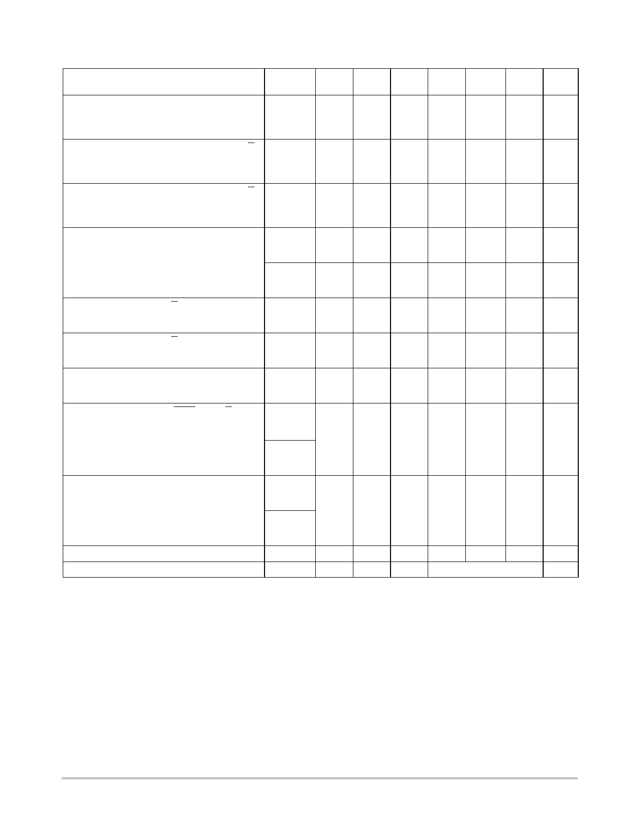
SWITCHING CHARACTERISTICS (CL = 50 pF, TA = 25_C) (Note 4)
Characteristic
CX
Symbol
pF
RX
VDD
Typ
kW
Vdc
Min (Note 5) Max Unit
Output Rise and Fall Time
tTLH, tTHL = (1.5 ns/pF) CL + 25 ns
tTLH, tTHL = (0.75 ns/pF) CL + 12.5 ns
tTLH, tTHL = (0.55 ns/pF) CL + 9.5 ns
tTLH,
−
−
ns
tTHL
5.0
−
100
200
10
−
50
100
15
−
40
80
Turn−Off, Turn−On Delay Time — A or B to Q or Q
tPLH, tPHL = (1.7 ns/pF) CL + 240 ns
tPLH, tPHL = (0.66 ns/pF) CL + 87 ns
tPLH, tPHL = (0.5 ns/pF) CL + 65 ns
tPLH,
tPHL
15
5.0
5.0
10
15
ns
−
325
650
−
120
240
−
90
180
Turn−Off, Turn−On Delay Time — A or B to Q or Q
tPLH,
1000
10
ns
tPLH, tPHL = (1.7 ns/pF) CL + 620 ns
tPHL
5.0
−
705
−
tPLH, tPHL = (0.66 ns/pF) CL + 257 ns
10
−
290
−
tPLH, tPHL = (0.5 ns/pF) CL + 185 ns
15
−
210
−
Input Pulse Width — A or B
tWH
15
5.0
5.0
150
70
−
ns
10
75
30
−
15
55
30
−
1000
10
5.0
−
70
−
ns
tWL
10
−
30
−
15
−
30
−
Output Pulse Width — Q or Q
(For CX < 0.01 mF use graph for
appropriate VDD level.)
Output Pulse Width — Q or Q
(For CX > 0.01 mF use formula:
tW = 0.2 RX CX Ln [VDD – VSS]) (Note 6)
Pulse Width Match between Circuits in the same
package
tW
15
5.0
5.0
−
550
−
ns
10
−
350
−
15
−
300
−
tW
10,000 10
5.0
15
30
45
ms
10
10
50
90
15
15
55
95
t1 – t2 10,000 10
5.0
−
6.0
25
%
10
−
8.0
35
15
−
8.0
35
Reset Propagation Delay — Reset to Q or Q
tPLH,
tPHL
15
5.0
5.0
10
15
1000
10
5.0
10
15
−
325
600
ns
−
90
225
−
60
170
−
1000
−
ns
−
300
−
−
250
−
Retrigger Time
15
5.0
5.0
0
−
−
ns
trr
10
0
−
−
15
0
−
−
1000
10
5.0
0
−
−
ns
10
0
−
−
15
0
−
−
External Timing Resistance
RX
−
−
−
5.0
−
1000 kW
External Timing Capacitance
CX
−
−
−
No Limits (Note 7)
mF
4. The formulas given are for the typical characteristics only at 25_C.
5. Data labelled “Typ” is not to be used for design purposes but is intended as an indication of the IC’s potential performance.
6. If CX > 15 mF, Use Discharge Protection Diode DX, per Figure 9.
7. RXis in W, CX is in farads, VDD and VSS in volts, PWout in seconds.
http://onsemi.com
4
Share Link: 