MAX104 View Datasheet(PDF) - Maxim Integrated
Part Name
Description
MFG CO.
MAX104 Datasheet PDF : 30 Pages
| |||
±5V, 1Gsps, 8-Bit ADC with
On-Chip 2.2GHz Track/Hold Amplifier
Table 4. Ideal Input Voltage and Output Code Results for Differential Operation
VIN+
+125mV
+125mV - 0.5LSB
0V
-125mV + 0.5LSB
-125mV
VIN-
-125mV
-125mV + 0.5LSB
0V
+125mV - 0.5LSB
+125mV
OVERRANGE BIT
1
0
0
0
0
OUTPUT CODE
11111111 (full scale)
11111111
01111111
toggles
10000000
00000001
00000000 (zero scale)
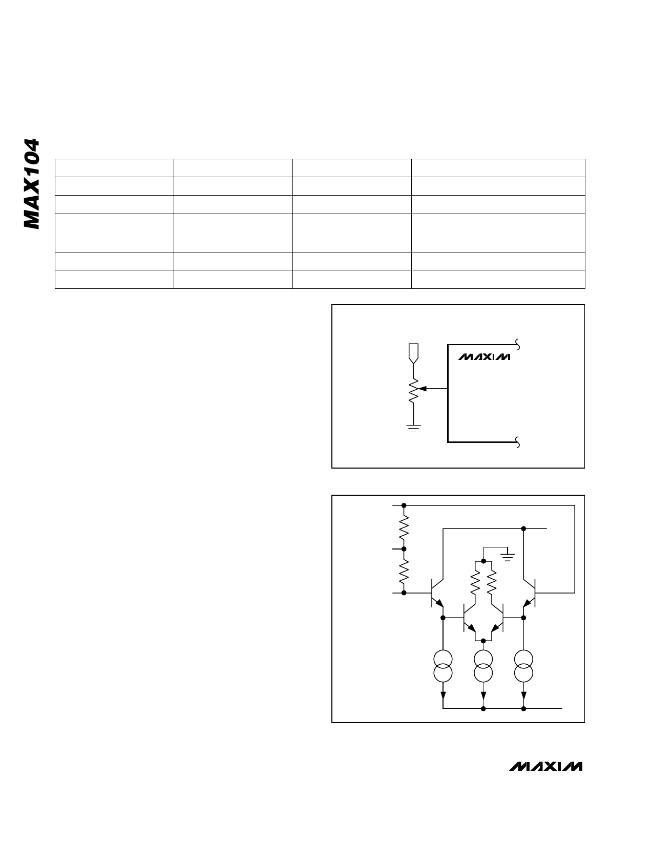
Offset Adjust
The MAX104 provides a control input (VOSADJ) to com-
pensate for system offsets. The offset adjust input is a
self-biased voltage divider from the internal +2.5V preci-
sion reference. The nominal open-circuit voltage is one-
half the reference voltage. With an input resistance of
typically 25kΩ, this pin may be driven by an external
10kΩ potentiometer (Figure 11) connected between
REFOUT and GNDI to correct for offset errors. This con-
trol provides a typical ±5.5LSB offset adjustment range.
Clock Operation
The MAX104 clock inputs are designed for either single-
ended or differential operation (Figure 12) with flexible
input drive requirements. Each clock input is terminated
with an on-chip, laser-trimmed 50Ω resistor to CLKCOM
(clock-termination return). The CLKCOM termination
voltage can be connected anywhere between ground
and -2V for compatibility with standard ECL drive levels.
The clock inputs are internally buffered with a preampli-
fier to ensure proper operation of the data converter
with even small-amplitude sine-wave sources. The
MAX104 was designed for single-ended, low-phase-
noise sine-wave clock signals with as little as 100mV
amplitude (-10dBm). This eliminates the need for an
external ECL clock buffer and its added jitter.
Single-Ended Clock Inputs (Sine-Wave Drive)
Excellent performance is obtained by AC- or DC-cou-
pling a low-phase-noise sine-wave source into a single
clock input (Figure 13a, Table 5). For proper DC bal-
ance, the undriven clock input should be externally
50Ω reverse-terminated to GNDI.
The dynamic performance of the data converter is
essentially unaffected by clock-drive power levels from
REFOUT
MAX104
POT
VOSADJ
10k
GNDI
Figure 11. Offset Adjust with External 10kΩ Potentiometer
CLK+
50Ω
CLKCOM
50Ω
CLK-
+0.8V
GNDI
CLOCK INPUTS ARE
ESD PROTECTED
(NOT SHOWN IN THIS
SIMPLIFIED DRAWING).
VEE
Figure 12. Simplified Clock Input Structure (Single-Ended/
Differential)
18 ______________________________________________________________________________________
Share Link: 