LV8042LG View Datasheet(PDF) - SANYO -> Panasonic
Part Name
Description
MFG CO.
LV8042LG Datasheet PDF : 29 Pages
| |||
LV8042LG
5ch ⋅ 6ch (PWM) Setting/7ch (constant-current) Reference Voltage Setting
Register No.
D0
D1
D2
D3
D4
D5
D6
D7
Data
1
1
0 or 1
0 or 1
0 or 1
0 or 1
0 or 1
0 or 1
Nomenclature
RG_SELECT 1
RG_SELECT 2
F/R5
DECAY5
F/R6
DECAY6
VSEN7_SELECT 1
VSEN7_SELECT 1
Functions
Register select 1
Register select 1
Forward/reverse setting
Current attenuation mode setting
Forward/reverse setting
Current attenuation mode setting
7ch constant-current reference voltage select 1
7ch constant-current reference voltage select 2
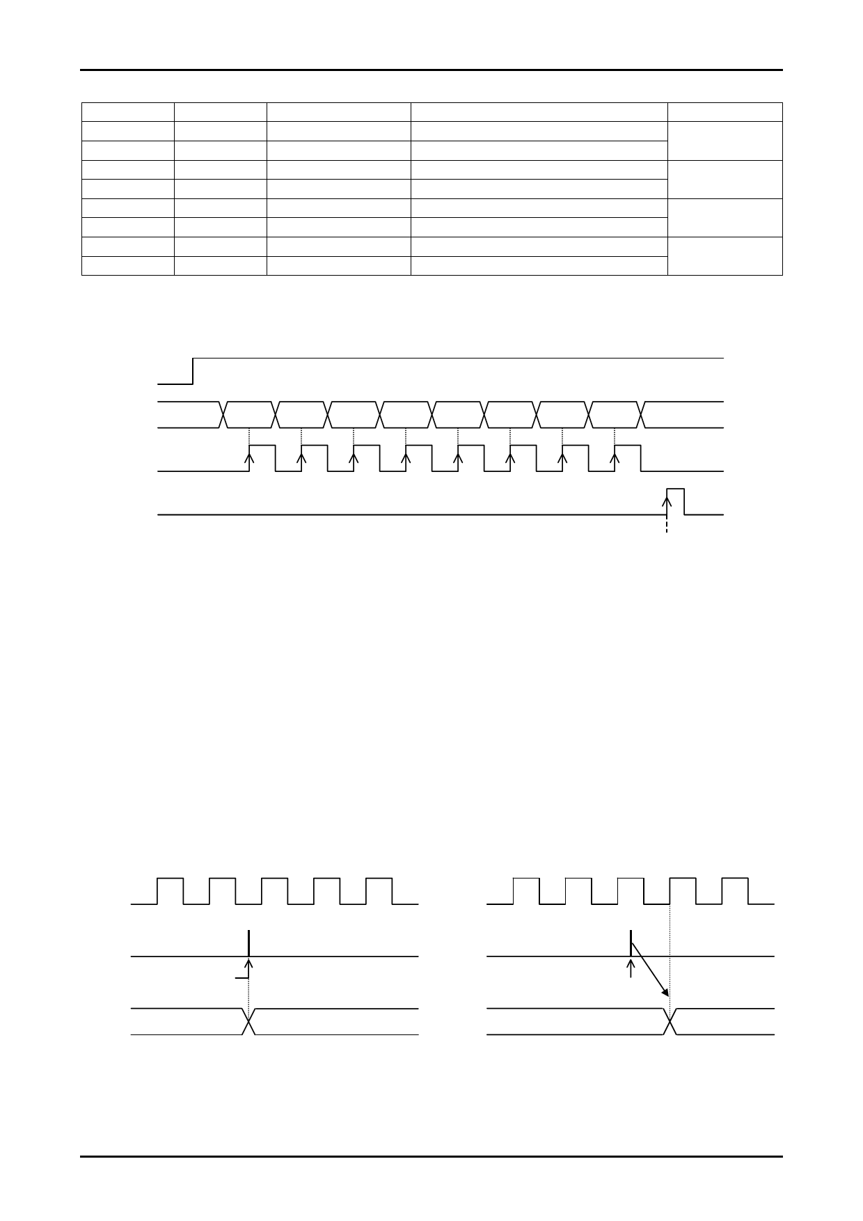
Serial Data Input Setting
Channel
5ch
PWM
6ch
PWM
7ch
Constant current
ST
DATA
SCLK
D0
D1
D2
D3
D4
D5
D6
D7
STB
Status setting data latched
Input DATA and SCLK after setting of STB = “L”. SCLK is not accepted in the state with STB = “H”.
Input DATA from D0 to D7 in this order. CLK performs data transmission at the rise edge and latches all data at rise
of STB after transmission of all data.
All of serial data is reset to “0” with ST = “L”. and at the voltage to cut VCC low voltage.
Timing to Reflect Serial Data to the Output
• PWM mode (Applicable to 3, 4, 5, and 6ch)
Type 1: FR and DECAY settings during PWM drive are reflected simultaneously with the STB signal of data
latching.
• STP mode (Applicable to 1, 2, 3, and 4ch)
Type 1: HOLD, RESET, CUT ENABLE settings and reference voltage setting are reflected simultaneously with the
STB signal of data latching.
Type 2: Forward/reverse (F/R) and excitation mode (MS) settings made during STEP setting are reflected at rise of the
next clock of data latching.
CLK
STB
Data latch timing
Type 1
STB timing
CLK
STB
Type 2
Data latch timing
Reflect at rise
Example: Two-phase excitation Example: phases excitation
No.A0004-11/29
Share Link: 