LTC6990CS6-PBF(V2) View Datasheet(PDF) - Linear Technology
Part Name
Description
MFG CO.
LTC6990CS6-PBF Datasheet PDF : 28 Pages
| |||
LTC6990
APPLICATIONS INFORMATION
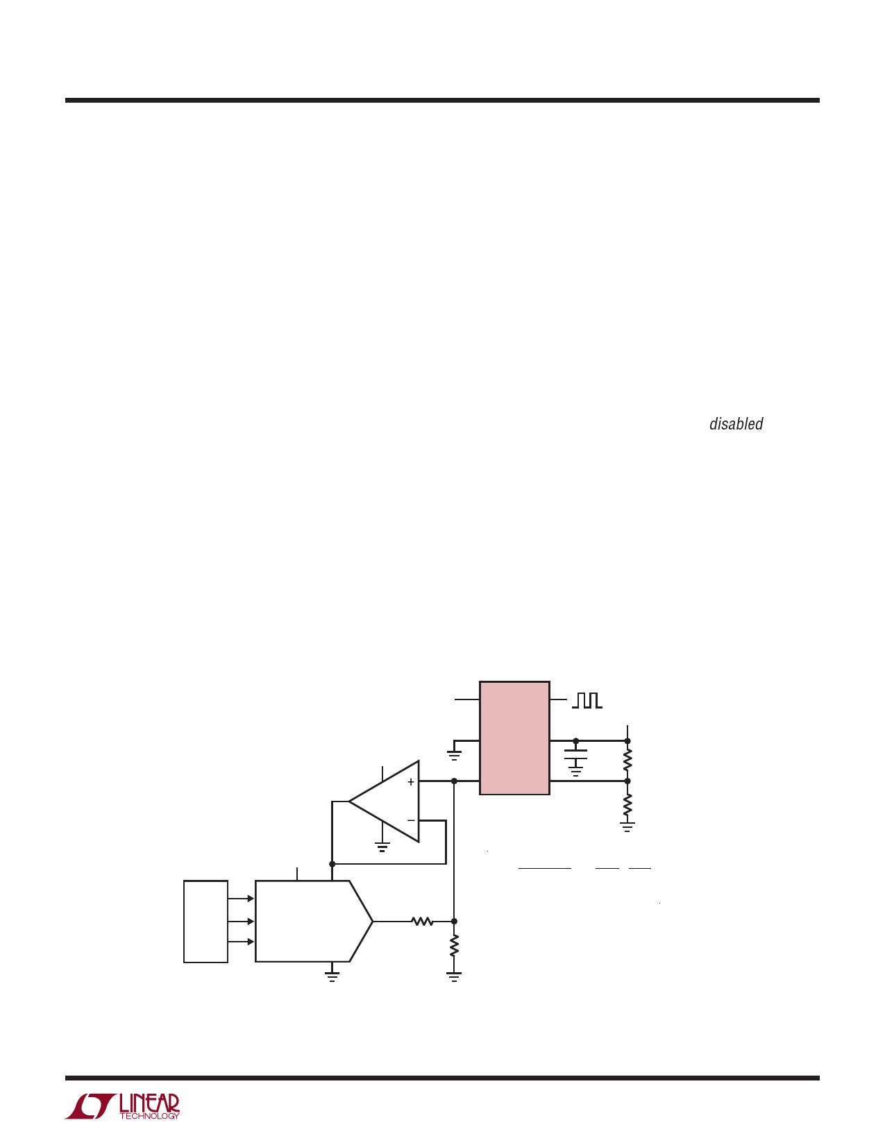
Eliminating VSET Error Effects with DAC Frequency
Control
Many DACs allow for the use of an external reference.
If such a DAC is used to provide the VCTRL voltage, the
VSET error is eliminated by buffering VSET and using it as
the DAC’s reference voltage, as shown in Figure 14. The
DAC’s output voltage now tracks any VSET variation and
eliminates it as an error source. The SET pin cannot be
tied directly to the reference input of the DAC because
the current drawn by the DAC’s REF input would affect
the frequency.
ISET Extremes (Master Oscillator Frequency Extremes)
Pushing ISET outside of the recommended 1.25μA to 20μA
range forces the master oscillator to operate outside of
the 62.5kHz to 1MHz range in which it is most accurate.
The oscillator will still function with reduced accuracy
in its extended range (see the Electrical Characteristics
section).
The LTC6990 is designed to function normally for ISET
as low as 1.25μA. At approximately 500nA, the oscillator
output will be frozen in its current state. For NDIV = 1 or 2,
OUT will halt in a low state. But for larger divider ratios,
it could halt in a high or low state. This avoids introduc-
ing short pulses while modulating a very low frequency
output. Note that the output will not be disabled as when
OE is low (e.g. the output will not enter a high impedance
state if Hi-Z = 1).
At the other extreme, the master oscillator frequency can
reach 2MHz for ISET = 40μA (RSET = 25k). It is not recom-
mended to operate the master oscillator beyond 2MHz
because the accuracy of the DIV pin ADC will suffer.
V+
1/2
LTC6078
OE
OUT
LTC6990
GND
V+
SET
DIV
6990 F14
V+
C1
0.1μF R1
R2
V+
DIN VCC
REF
RVCO
μP
CLK LTC1659 VOUT
fOUT
1MHz
NDIV
• 50k7
• RVCO
•
¥
§¦
1
RVCO
RSET
DIN ´
4096 ¶µ
DIN = 0 to 4095
CS/LD
GND
RSET
Figure 14. Digitally Controlled Oscillator with VSET Variation Eliminated
6990f
19
Share Link: 