5507 View Datasheet(PDF) - Linear Technology
Part Name
Description
MFG CO.
5507 Datasheet PDF : 8 Pages
| |||
LTC5507
PI FU CTIO S
SHDN (Pin 1): Shutdown Input. A logic low or no-connect
on the SHDN pin places the part in shutdown mode. A logic
high enables the part. SHDN has an internal 150k pull
down resistor to ensure that the part is in shutdown when
the enable driver is in a tri-state condition.
GND (Pin 2): System Ground.
VOUT (Pin 3): Buffered and Level Shifted Detector Output
Voltage.
VCC (Pin 4): Power Supply Voltage, 2.7V to 6V. VCC should
be bypassed with 0.1µF and 100pF ceramic capacitors.
PCAP (Pin 5): Peak Detector Hold Capacitor. Capacitor
value is dependent on RF frequency. Capacitor must be
connected between PCAP and VCC.
RFIN (Pin 6): RF Input Voltage. Referenced to VCC. A
coupling capacitor must be used to connect to the RF
signal source. This pin has an internal 250Ω termination
and an internal Schottky diode detector.
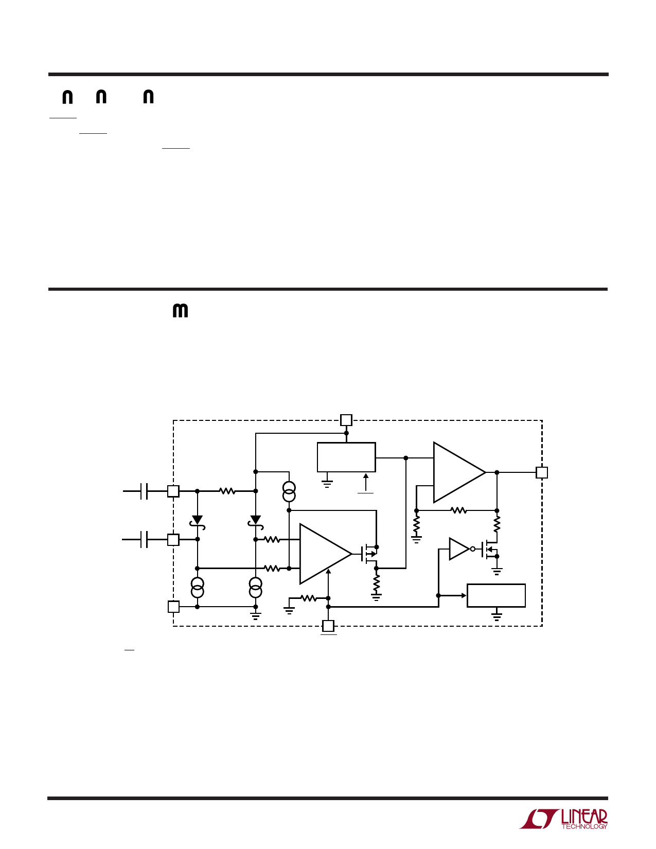
BLOCK DIAGRA
VCC
4
RFSOURCE
C1
6
RFIN
250Ω
GAIN
COMPRESSION
SHDN
C2
VCC
5
PCAP
GND 2
60µA
60µA
C1 = C2
C2 (µF) ≥ 1 , f = LOWEST RF INPUT FREQUENCY (MHz)
30f
+
RF DET
–
150k
1
SHDN
Figure 2.
+
BUFFER
–
30k
30k
3 VOUT
100Ω
BIAS
5507 BD
5507f
4
Share Link: 