LTC3406AIS5 View Datasheet(PDF) - Linear Technology
Part Name
Description
MFG CO.
LTC3406AIS5 Datasheet PDF : 16 Pages
| |||
LTC3406A
PIN FUNCTIONS
RUN (Pin 1): Run Control Input. Forcing this pin above 1.5V
enables the part. Forcing this pin below 0.3V shuts down
the device. In shutdown, all functions are disabled drawing
<1μA supply current. Do not leave RUN floating.
GND (Pin 2): Ground Pin.
SW (Pin 3): Switch Node Connection to Inductor. This pin
connects to the drains of the internal main and synchronous
power MOSFET switches.
VIN (Pin 4): Main Supply Pin. Must be closely decoupled to
GND, Pin 2, with a 2.2μF or greater ceramic capacitor.
VFB (Pin 5): Feedback Pin. Receives the feedback voltage
from an external resistive divider across the output.
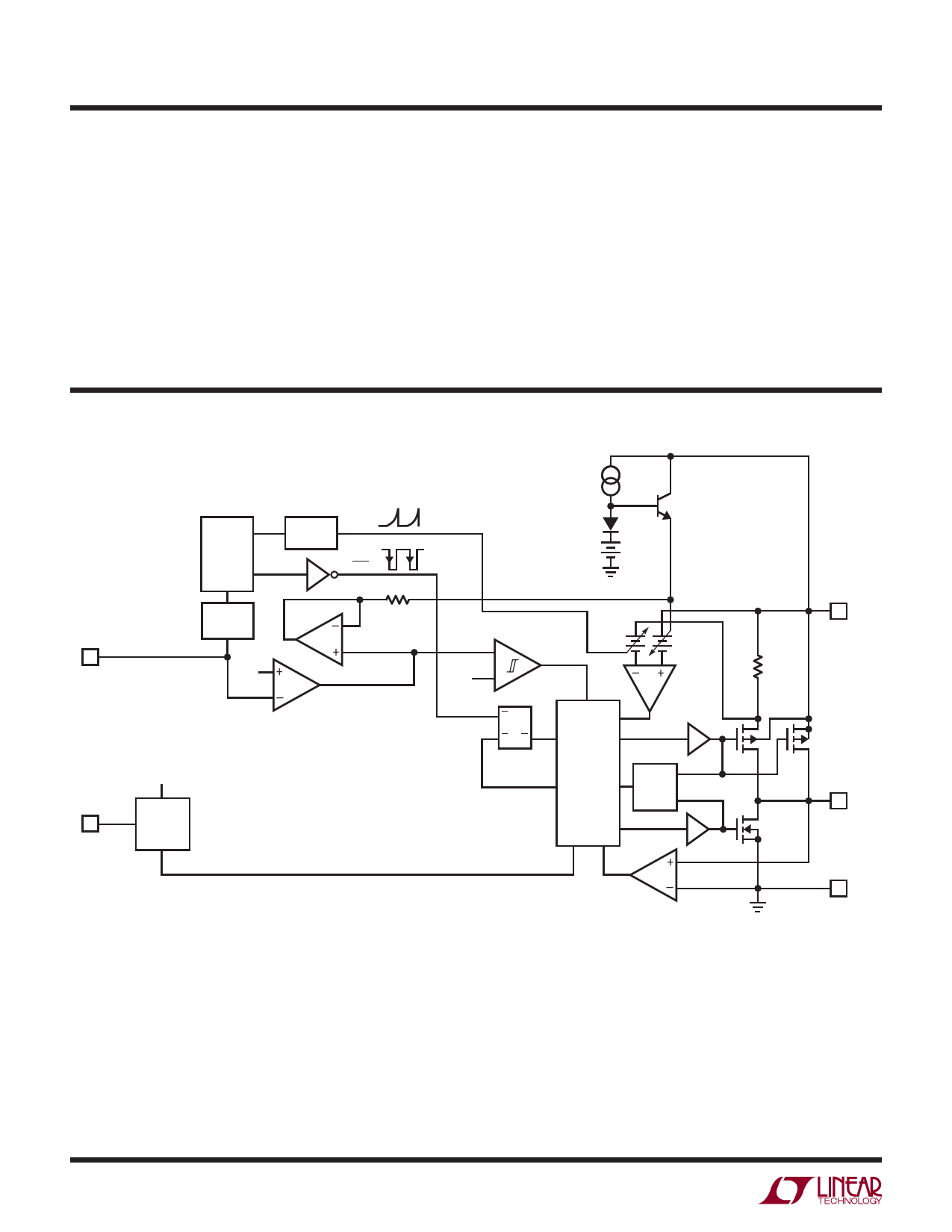
FUNCTIONAL DIAGRAM
SLOPE
COMP
OSC
OSC
FREQ
SHIFT
VFB
5
+
0.6V
– EA
VIN
RUN
1
0.6V REF
SHUTDOWN
0.65V
–
SLEEP
0.4V
+
BURST
ICOMP
SQ
RQ
RS LATCH
SWITCHING
LOGIC
AND
BLANKING
CIRCUIT
ANTI-
SHOOT-
THRU
IRCMP
4 VIN
5Ω
3 SW
2 GND
3406A BD
3406afa
6
Share Link: 