LTC1090ACN View Datasheet(PDF) - Linear Technology
Part Name
Description
MFG CO.
LTC1090ACN Datasheet PDF : 28 Pages
| |||
LTC1090
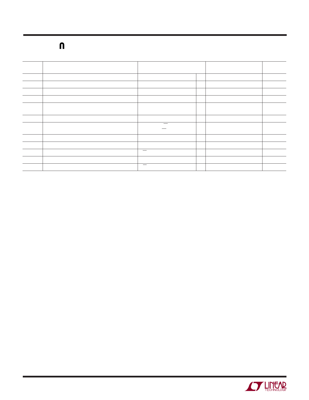
DIGITAL A D DC ELECTRICAL CHARACTERISTICS The ● denotes specifications which apply
over the full operating temperature range, otherwise specification are TA = 25°C. (Note 3)
SYMBOL PARAMETER
CONDITIONS
LTC1090/LTC1090A
MIN
TYP
MAX
UNITS
VIH
VIL
IIH
IIL
VOH
VOL
IOZ
ISOURCE
ISINK
ICC
IREF
I–
High Level lnput Voltage
Low Level Input Voltage
High Level lnput Current
Low Level Input Current
High Level Output Voltage
Low Level Output Voltage
Hi-Z Output Leakage
Output Source Current
Output Sink Current
Positive Supply Current
Reference Current
Negative Supply Current
VCC = 5.25V
● 2.0
V
VCC = 4.75V
●
0.8
V
VIN = VCC
●
2.5
µA
VIN = 0V
●
–2.5
µA
VCC = 4.75V, lO = 10µA
4.7
V
VCC = 4.75V, lO = 360µA
● 2.4
4.0
V
VCC = 4.75V, lO = 1.6mA
●
0.4
V
VOUT = VCC, CS High
●
VOUT = 0V, CS High
●
3
µA
–3
µA
VOUT = 0V
– 10
mA
VOUT = VCC
CS High, REF+ Open
●
10
mA
1.0
2.5
mA
VREF = 5V
●
CS High, V– = – 5V
●
0.5
1.0
mA
1
50
µA
Note 1: Absolute Maximum Ratings are those values beyond which the life
of a device may be impaired.
Note 2: All voltage values are with respect to ground with DGND, AGND
and REF– wired together (unless otherwise noted).
Note 3: VCC = 5V, VREF + = 5V, VREF – = 0V, V– = 0V for unipolar mode and
–5V for bipolar mode, ACLK = 2.0MHz, SCLK = 0.5MHz unless otherwise
specified.
Note 4: These specs apply for both unipolar and bipolar modes. In bipolar
mode, one LSB is equal to the bipolar input span (2VREF) divided by 1024.
For example, when VREF = 5V, 1LSB (bipolar) = 2(5V)/1024 = 9.77mV.
Note 5: Linearity error is specified between the actual end points of the
A/D transfer curve.
Note 6: Total unadjusted error includes offset, gain, linearity, multiplexer
and hold step errors.
Note 7: Two on-chip diodes are tied to each reference and analog input
which will conduct for reference or analog input voltages one diode drop
below V– or one diode drop above VCC. Be careful during testing at low
VCC levels (4.5V), as high level reference or analog inputs (5V) can cause
this input diode to conduct, especially at elevated temperatures, and cause
errors for inputs near full-scale. This spec allows 50mV forward bias of
either diode. This means that as long as the reference or analog input does
not exceed the supply voltage by more than 50mV, the output code will be
correct. To achieve an absolute 0V to 5V input voltage range will therefore
require a minimum supply voltage of 4.950V over initial tolerance,
temperature variations and loading.
Note 8: Channel leakage current is measured after the channel selection.
Note 9: To minimize errors caused by noise at the chip select input, the
internal circuitry waits for two ACLK falling edges after a chip select falling
edge is detected before responding to control input signals. Therefore, no
attempt should be made to clock an address in or data out until the
minimum chip select setup time has elapsed.
1090fc
4
Share Link: 