IMP802L View Datasheet(PDF) - A1 PROs co., Ltd.
Part Name
Description
MFG CO.
IMP802L Datasheet PDF : 10 Pages
| |||
IMP690A, 692A, 802L, 802M, 805L
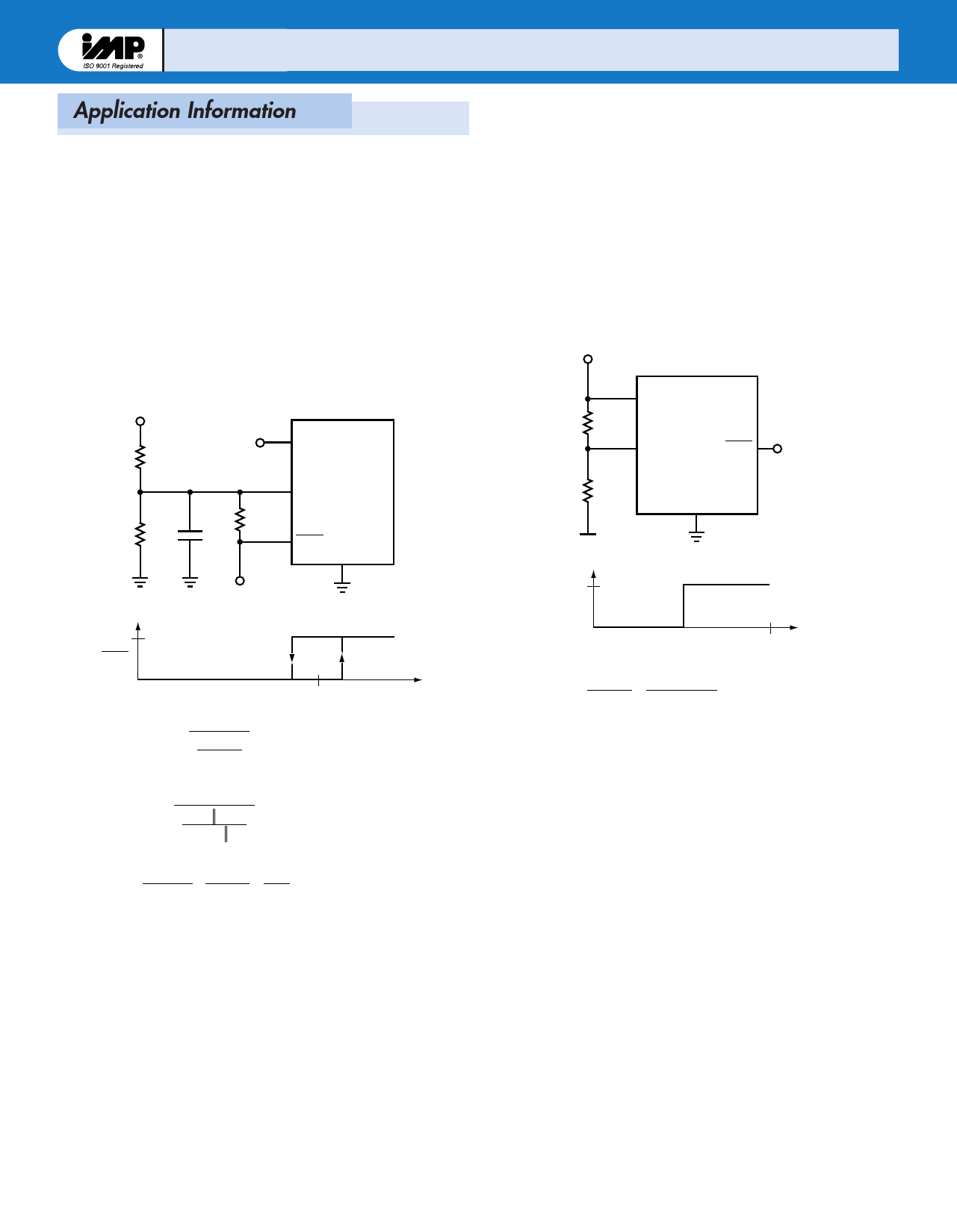
Application Information
Power Fail Hysteresis
A noise margin can be added to the simple monitoring circuit of
Figure 7 by adding positive feedback from thePFO pin. The cir-
cuit of Figure 8 adds this positive “latching” effect by means of an
additional resistor R3 connected betweenPFO and PFI which
helps in pulling PFI in the direction ofPFO and eliminating an
indecision at the trip point. Resistor R3 is normally about 10 times
higher in resistance than R2 to keep the hysteresis band reason-
able and should be larger than 10kΩ to avoid excessive loading on
thePFO pin. The calculations for the correct values of resistors to
set the hysteresis thresholds are given in Figure 8. A capacitor can
be added to offer additional noise rejection by low-pass filtering.
Monitoring Capabilities of the Power-Fail Input
Although designed for power supply failure monitoring, the PFI
pin can be used for monitoring any voltage condition that can be
scaled by means of a resistive divider. An example is the negative
power supply monitor configured in Figure 9. In this case a good
negative supply will hold the PFI pin below 1.25V and thePFO
pin will be at a logic “0”. As the negative voltage declines,
the voltage at the PFI pin will rise until it exceeds 1.25V and
thePFO pin will go to a logic “1”.
+5V
VIN
R1
R2
+5V
R3
C1*
VCC
IMP690A
IMP692A
PFI
IMP802L
IMP802M
IMP805L
PFO
GND
VCC
IMP690A
R1
IMP692A
PFI
IMP802L
IMP802M
PFO
IMP805L
R2
GND
V–
V– = VTRIP
To µP
+5V
PFO
0V
0V
V TRIP =
1.25
R
R2
2+R
2
*Optional
VL VTRIP VH
VIN
+5V
PFO
0V
VTRIP
V–
5 − 1.25 = 1.25 − VTRIP
R1
R2
0V
690A_11.eps
Figure 9. Using PFI to monitor negative supply voltage
VIH =
1.25
R2 R3
R1+ R 2 R 3
V L− 1.25 + 5 − 1.25 = 1.25
R1
R3
R2
690A_10.eps
Figure 8. Hysteresis added to PFI pin
8
Share Link: 