IDT82V3002A View Datasheet(PDF) - Integrated Device Technology
Part Name
Description
MFG CO.
IDT82V3002A Datasheet PDF : 28 Pages
| |||
IDT82V3002A WAN PLL WITH DUAL REFERENCE INPUTS
INDUSTRIAL TEMPERATURE RANGE
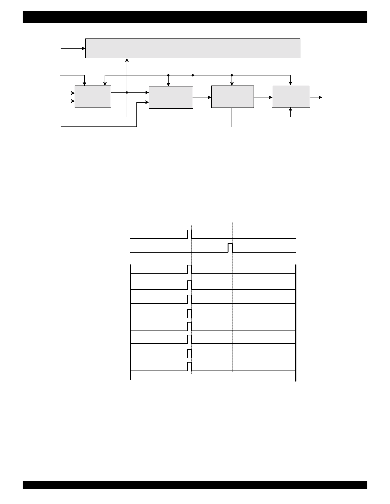
TIE_en
Step Generation
IN_sel
Fref0
Fref1
Select
Circuit
Fref
Measure
Circuit
Storage
Circuit
Trigger
Circuit
Virtual
Reference
Signal
Feedback
signal
TCLR
Figure - 5 TIE Control Circuit Diagram
The TIE Control Block will work under the control of the Step
Generation circuit when it is enabled manually or automatically (by the
TIE_en pin or TIE auto-enable logic generated by the State Control
Circuit).
The selected reference signal is compared with the feedback signal
(current output feedback from the Frequency Select Circuit) by the
Measure Circuit. The phase difference between the input reference and
the feedback signal is sent to the Storage Circuit for TIE correction. The
Trigger Circuit generates a virtual reference with the phase corrected to
the same position as the previous reference according to the value
stored in the Storage Circuit. With this TIE correction mechanism, the
reference is switched without generating a step change in phase.
Figure - 6 shows the phase transient that would result if a reference
switch is performed with the TIE Control Block enabled.
Fref0
Fref1
Time = 0.00 s
Time = 0.25 s
Time = 0.50 s
Time = 0.75 s
Time = 1.0 s
Time = 1.25 s
Time = 1.50 s
Time = 1.75 s
Input Clock
Output Clock
Figure - 6 Reference Switch with TIE Control Block Enabled
The phase difference in the Storage Circuit can be cleared by
applying a logic low pulse to the TCLR pin. The reset pulse should be at
least 300 ns.
When the IDT82V3002A primarily enters Holdover Mode for short
time periods and then turns back to Normal Mode, the TIE Control
Circuit should not be enabled. This will prevent undesired accumulated
phase change between the input and output.
If the TIE Control Block is disabled manually or automatically during
the reference switching, the phase of the output signal will align with that
of the new reference. The phase slope is limited to 5 ns per 125 µs.
Figure - 7 shows the phase transient resulting from a reference switch
with the TIE Control Block disabled.
13
Share Link: 