IDT72205LB10PFI8(2017) View Datasheet(PDF) - Integrated Device Technology
Part Name
Description
MFG CO.
IDT72205LB10PFI8
(Rev.:2017)
(Rev.:2017)
Integrated Device Technology
IDT72205LB10PFI8 Datasheet PDF : 16 Pages
| |||
IDT72205LB/72215LB/72225LB/72235LB/72245LB CMOS SyncFIFOTM
256 x 18, 512 x 18, 1,024 x 18, 2,048 x 18 and 4,096 x 18
COMMERCIAL AND INDUSTRIAL
TEMPERATURE RANGES
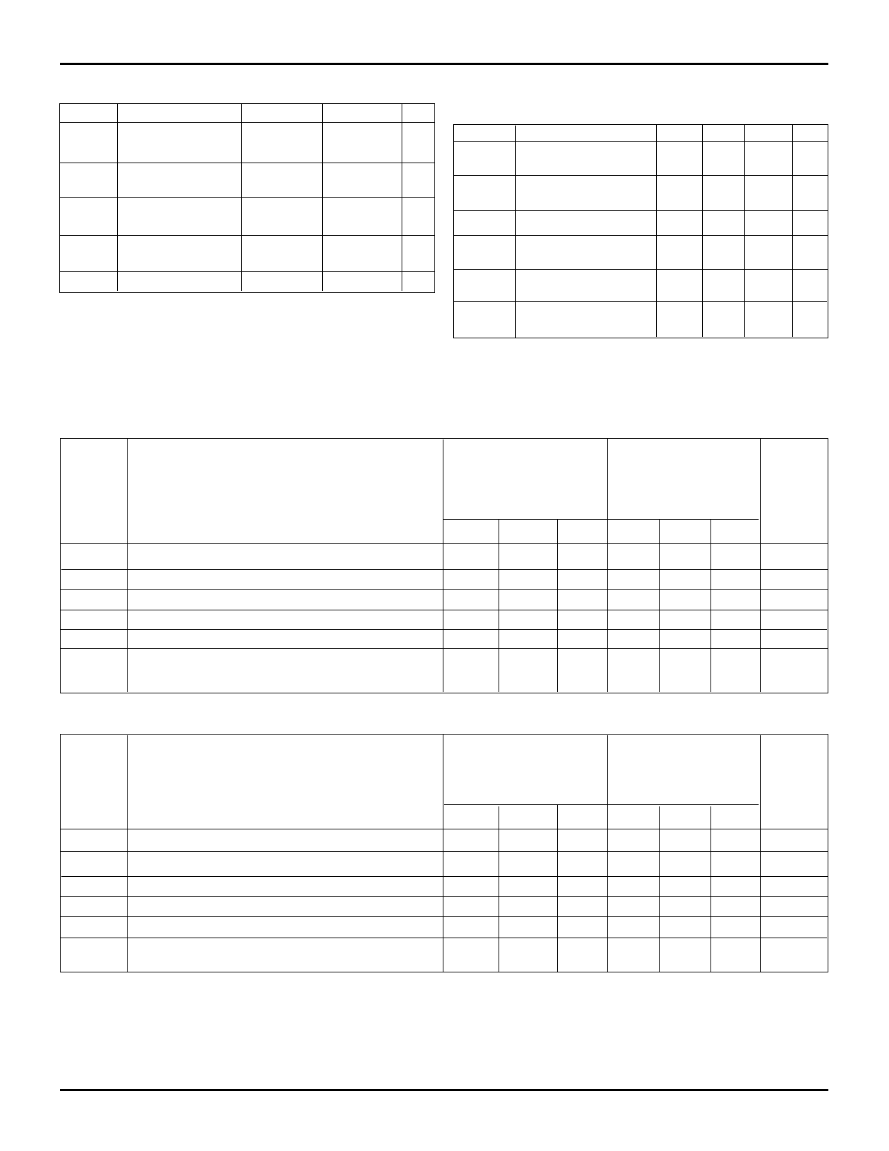
AC ELECTRICAL CHARACTERISTICS
(Commercial: VCC = 5V ± 10%, TA = 0°C to +70°C; Industrial: VCC = 5V ± 10%, TA = -40°C to +85°C)
Commercial
Commercial & Industrial(1)
IDT72205LB10
IDT72215LB10
IDT72225LB10
IDT72235LB10
IDT72245LB10
IDT72205LB15
IDT72215LB15
IDT72225LB15
IDT72235LB15
IDT72245LB15
IDT72205LB25
IDT72215LB25
IDT72225LB25
IDT72235LB25
IDT72245LB25
Symbol
Parameter
Min.
Max.
Min.
Max.
Min.
Max. Unit
fS
Clock Cycle Frequency
—
tA
Data Access Time
2
tCLK
Clock Cycle Time
10
tCLKH
Clock HIGH Time
4.5
tCLKL
Clock LOW Time
4.5
tDS
Data Set-up Time
3
tDH
Data Hold Time
0
tENS
Enable Set-up Time
3
tENH
Enable Hold Time
0
tRS
Reset Pulse Width(2)
10
tRSS
Reset Set-up Time
8
tRSR
Reset Recovery Time
8
tRSF
Reset to Flag and Output Time
—
tOLZ
Output Enable to Output in Low-Z(3)
0
tOE
Output Enable to Output Valid
3
tOHZ
Output Enable to Output in High-Z(3)
3
tWFF
Write Clock to Full Flag
—
tREF
Read Clock to Empty Flag
—
tPAF
Clock to Asynchronous Programmable Almost-Full Flag
—
tPAE
Clock to Programmable Almost-Empty Flag
—
tHF
Clock to Half-Full Flag
—
tXO
Clock to Expansion Out
—
tXI
Expansion In Pulse Width
3
tXIS
Expansion In Set-Up Time
3.5
tSKEW1 Skew time between Read Clock & Write Clock forFull Flag
5
tSKEW2(2) Skew time between Read Clock & Write Clock for Empty Flag
5
100
—
6.5
2
—
15
—
6
—
6
—
4
—
1
—
4
—
1
—
15
—
10
—
10
15
—
—
0
6
3
6
3
6.5
—
6.5
—
17
—
17
—
17
—
6.5
—
—
6.5
—
5
—
6
—
6
66.7
—
10
2
—
25
—
10
—
10
—
6
—
1
—
6
—
1
—
25
—
15
—
15
20
—
—
0
8
3
8
3
10
—
10
—
24
—
24
—
24
—
10
—
—
10
—
10
—
10
—
10
40
MHz
15
ns
—
ns
—
ns
—
ns
—
ns
—
ns
—
ns
—
ns
—
ns
—
ns
—
ns
25
ns
—
ns
12
ns
12
ns
15
ns
15
ns
26
ns
26
ns
26
ns
15
ns
—
ns
—
ns
—
ns
—
ns
NOTES:
1. Industrial temperature range product for the 15ns and the 25ns speed grades are available as a standard device. All other speed grades are available by special order.
2. Pulse widths less than minimum values are not allowed.
3. Values guaranteed by design, not currently tested.
AC TEST CONDITIONS
Input Pulse Levels
Input Rise/Fall Times
Input Timing Reference Levels
Output Reference Levels
Output Load
GND to 3.0V
3ns
1.5V
1.5V
See Figure 1
D.U.T.
680Ω
5V
1.1K
30pF*
2766 drw 04
Figure 1. Output Load
* Includes jig and scope capacitances.
5
MARCH 2013
Share Link: 