GS70328TS-10IT View Datasheet(PDF) - Giga Semiconductor
Part Name
Description
MFG CO.
GS70328TS-10IT Datasheet PDF : 11 Pages
| |||
GS70328SJ/TS
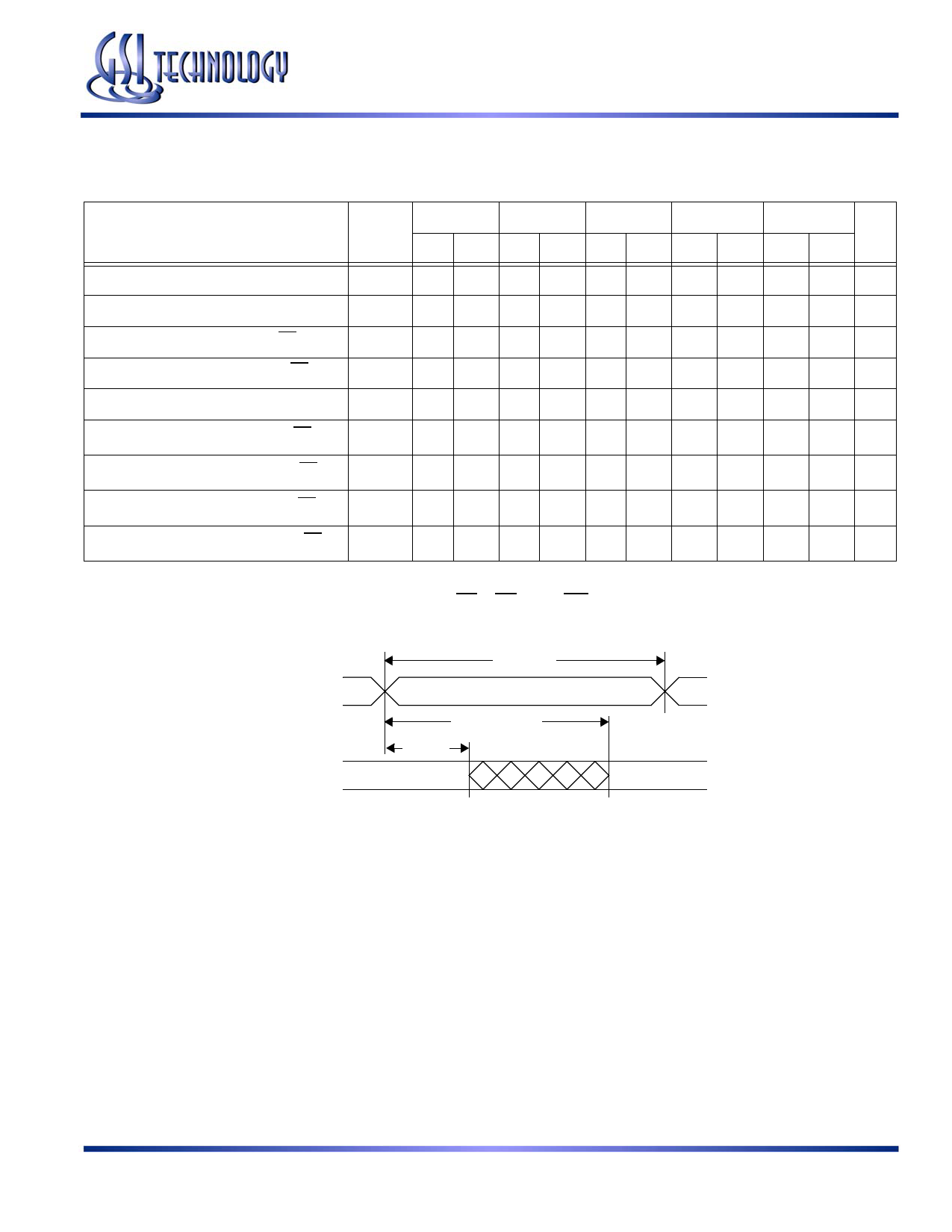
AC Characteristics
Read Cycle
Parameter
-7
-8
-10
-12
-15
Symbol
Unit
Min Max Min Max Min Max Min Max Min Max
Read cycle time
tRC
7 — 8 — 10 — 12 — 15 — ns
Address access time
tAA
— 7 — 8 — 10 — 12 — 15 ns
Chip enable access time (CE)
tAC
— 7 — 8 — 10 — 12 — 15 ns
Output enable to output valid (OE)
tOE — 3.5 — 4 — 5 — 6 — 7 ns
Output hold from address change
tOH
2 — 2 — 2 — 3 — 3 — ns
Chip enable to output in low Z (CE)
tLZ*
2 — 2 — 2 — 3 — 3 — ns
Output enable to output in low Z (OE)
tOLZ*
0—0—0—
0
—
0
— ns
Chip disable to output in High Z (CE)
tHZ*
— 3.5 — 4 — 5
—
6
—
7 ns
Output disable to output in High Z (OE)
tOHZ*
—
3 — 3.5 —
4
—
5
—
6
ns
* These parameters are sampled and are not 100% tested
Read Cycle 1: CE = OE = VIL, WE = VIH
Address
Data Out
tOH
Previous Data
tRC
tAA
Data valid
Rev: 1.11 11/2004
5/11
Specifications cited are subject to change without notice. For latest documentation see http://www.gsitechnology.com.
© 1999, GSI Technology
Share Link: 