FSBM10SM60A View Datasheet(PDF) - Fairchild Semiconductor
Part Name
Description
MFG CO.
FSBM10SM60A Datasheet PDF : 16 Pages
| |||
Gating W H
Gating VH
C
P
Gating UH
U
F a u lt
Gating W H
Gating VH
Gating UH
15V line
RS
RS
RS
RS
RS
RS
RS
C B PF
5V line
RPH
CPH
RPH
CPH
5V line
RPH
CPH
RPL RPL RPL RPF
CPL CPL CPL CPF
RBS
DBS
CBS
CBSC
RBS
DBS
CBS CBSC
RBS
DBS
CBS
RSC
CBSC
RF
CSC
RCSC
CFOD
(22) VB(W)
(21) V CC(WH)
(20) IN (WH)
(23) VS(W)
(18) VB(V)
(17) V CC(VH)
(16) COM(H)
(15) IN (VH)
(19) VS(V)
(13) VB(U)
(12) V CC(UH)
(11) IN (UH)
(14) VS(U)
(10) RSC
(9) CSC
(8) CFOD
(7) VFO
(6) COM (L)
(5) IN (WL)
(4) IN (VL)
(3) IN (UL)
(2) COM(L)
(1) VCC(L)
CSP15
CSPC15
VB
VCC
COM
IN
OUT
VS
VB
VCC
COM
IN
OUT
VS
VB
VCC
COM
IN
OUT
VS
C(SC) O UT(W L)
C(FO D)
VFO
IN(WL) OUT(VL)
IN (VL )
IN (U L)
COM(L)
O UT(UL )
VCC
W-Phase Current
V-Phase Current
U-Phase Current
P (32)
W (31)
V (30)
U (29)
NW (28)
NV (27)
NU (26)
NC (24)
NC (25)
R FW
R FV
R FU
CFW
C FV
CFU
M
CDCS
Vdc
RSW
RSV
RSU
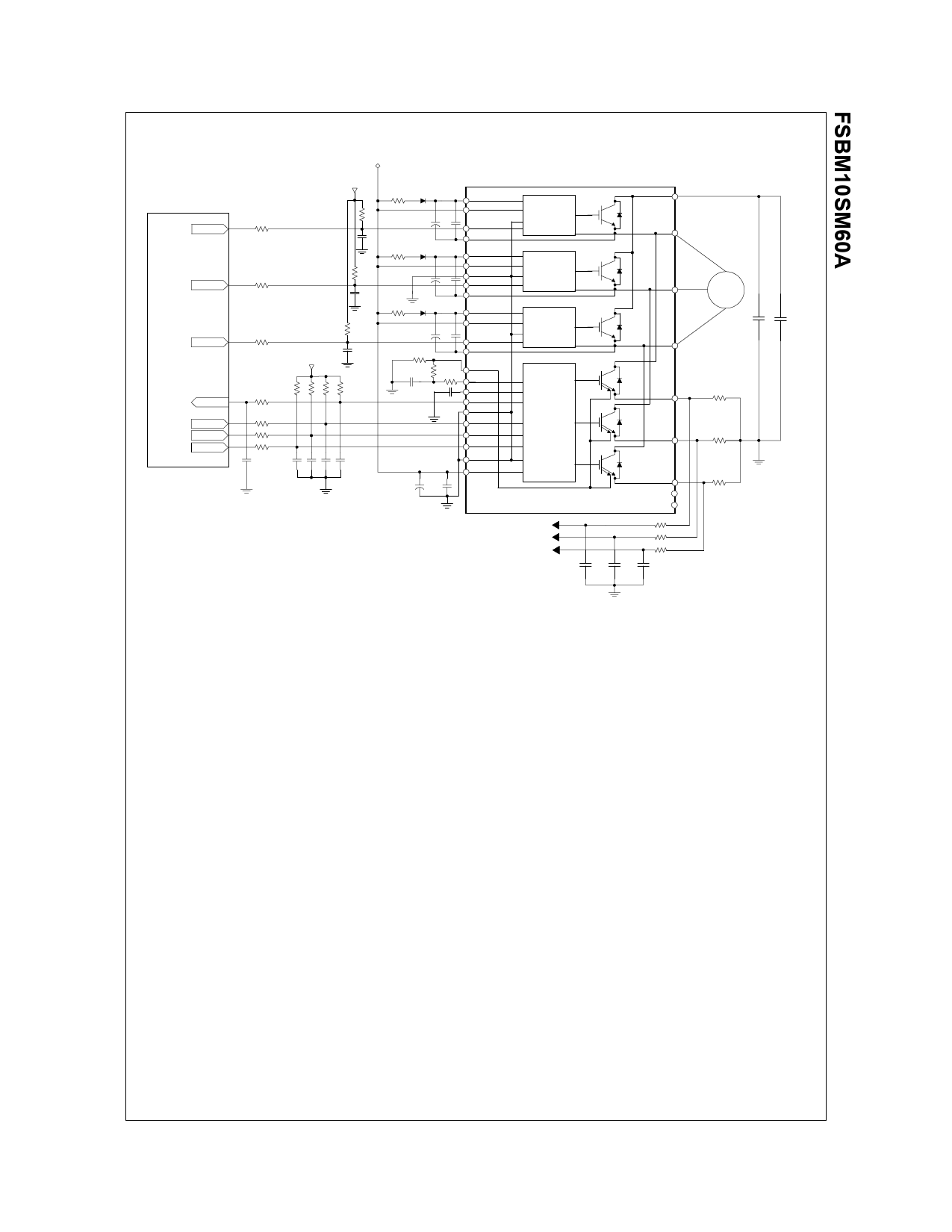
Note:
1) RPLCPL/RPHCPH /RPFCPF coupling at each SPM input is recommended in order to prevent input signals’ oscillation and it should be as close as possible to each
SPM input pin.
2) By virtue of integrating an application specific type HVIC inside the SPM, direct coupling to CPU terminals without any opto-coupler or transformer isolation is
possible.
3) VFO output is open collector type. This signal line should be pulled up to the positive side of the 5V power supply with approximately 4.7kΩ resistance. Please
refer to Fig. 14.
4) CSP15 of around 7 times larger than bootstrap capacitor CBS is recommended.
5) VFO output pulse width should be determined by connecting an external capacitor(CFOD) between CFOD(pin8) and COM(L)(pin2). (Example : if CFOD = 33 nF, then
tFO = 1.8 ms (typ.)) Please refer to the note 6 for calculation method.
6) Each input signal line should be pulled up to the 5V power supply with approximately 4.7kΩ (at high side input) or 2kΩ (at low side input) resistance (other RC
coupling circuits at each input may be needed depending on the PWM control scheme used and on the wiring impedance of the system’s printed circuit board).
Approximately a 0.22~2nF by-pass capacitor should be used across each power supply connection terminals.
7) To prevent errors of the protection function, the wiring around RSC, RF and CSC should be as short as possible.
8) In the short-circuit protection circuit, please select the RFCSC time constant in the range 3~4 µs.
9) To enhance the noise immunity, CSC pin should be connected to the external circuit through a series resistor, RCSC, which is approximately 390Ω. RSCS should
be connected to CSC pin as close as possible.
10)Each capacitor should be mounted as close to the pins of the SPM as possible.
11)To prevent surge destruction, the wiring between the smoothing capacitor and the P&N pins should be as short as possible. The use of a high frequency non-
inductive capacitor of around 0.1~0.22 uF between the P&N pins is recommended.
12)Relays are used at almost every systems of electrical equipments of home appliances. In these cases, there should be sufficient distance between the CPU and
the relays. It is recommended that the distance be 5cm at least.
Fig. 14. Typical Application Circuit
©2003 Fairchild Semiconductor Corporation
Rev. E, August 2003
Share Link: 