FSBM10SM60A View Datasheet(PDF) - Fairchild Semiconductor
Part Name
Description
MFG CO.
FSBM10SM60A Datasheet PDF : 16 Pages
| |||
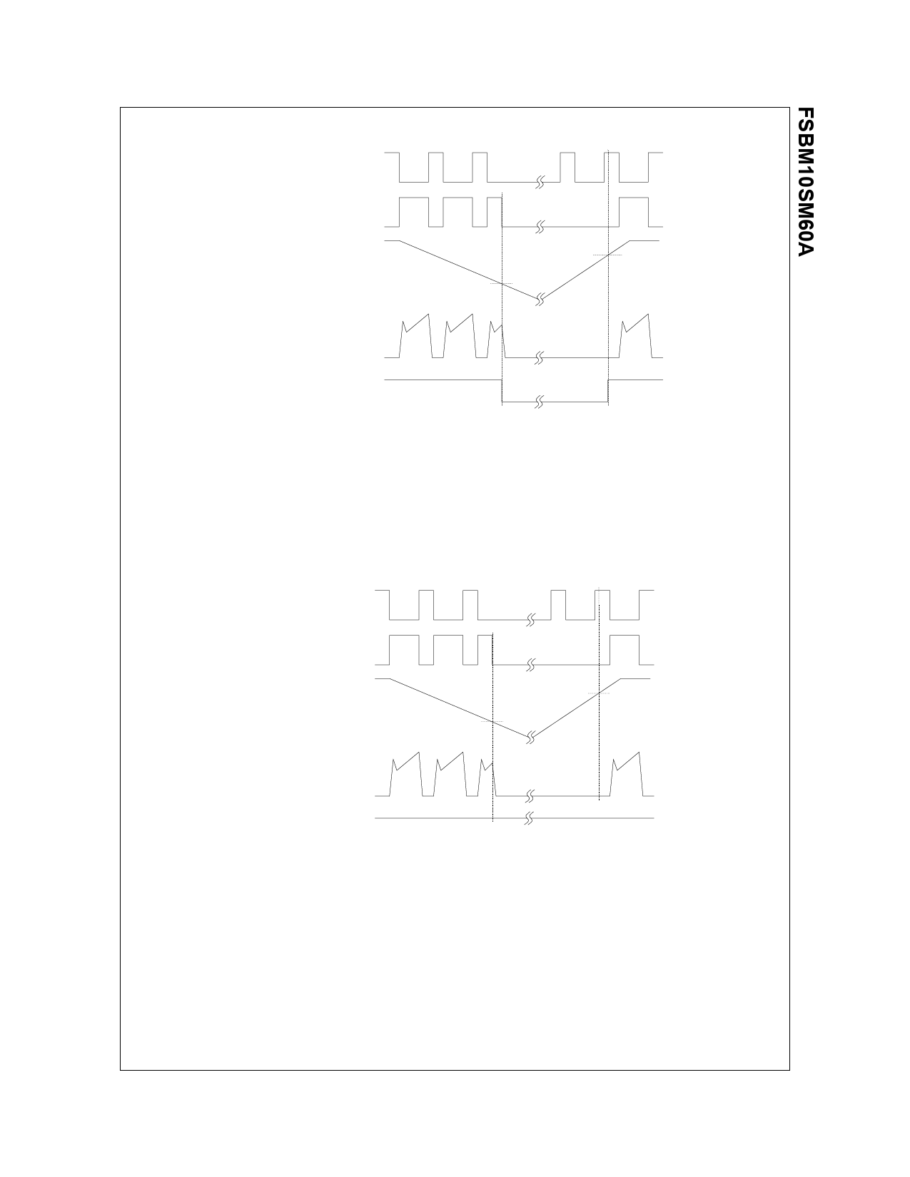
Time Charts of SPMs Protective Function
Input Signal
Internal IGBT
Gate-Emitter Voltage
Control Supply Voltage
Output Current
P3
P2
UV detect
P1
P5 UV reset
P6
Fault Output Signal
P4
P1 : Normal operation - IGBT ON and conducting current
P2 : Under-Voltage detection
P3 : IGBT gate interrupt
P4 : Fault signal generation
P5 : Under-Voltage reset
P6 : Normal operation - IGBT ON and conducting current
Fig. 9. Under-Voltage Protection (Low-side)
Input Signal
VB S
Output Current
P3
P2
UV detect
P1
P5 UV reset
P6
Fault Output Signal
P4
P1 : Normal operation - IGBT ON and conducting current
P2 : Under-Voltage detection
P3 : IGBT gate interrupt
P4 : No fault signal
P5 : Under-Voltage reset
P6 : Normal operation - IGBT ON and conducting current
Fig. 10. Under-Voltage Protection (High-side)
©2003 Fairchild Semiconductor Corporation
Rev. E, August 2003
Share Link: 