CY7C4275V-15(2001) View Datasheet(PDF) - Cypress Semiconductor
Part Name
Description
MFG CO.
CY7C4275V-15 Datasheet PDF : 20 Pages
| |||
CY7C4255V/CY7C4265V
CY7C4275V/CY7C4285V
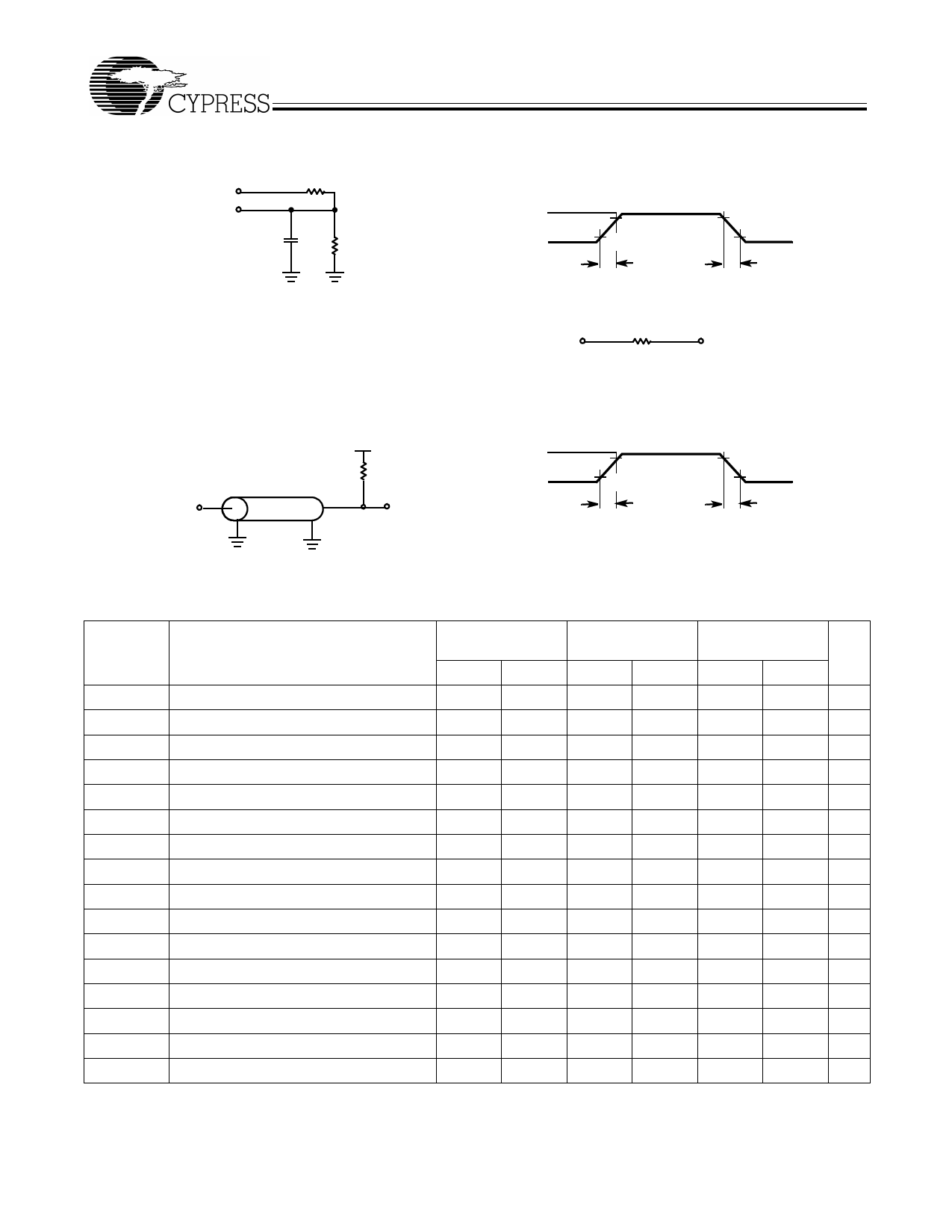
AC Test Loads and Waveforms (-15 -25)[8, 9]
3.3V
OUTPUT
R1=330Ω
CL
INCLUDING
JIG AND
SCOPE
R2=510Ω
4275V–4
3.0V
GND
≤ 3 ns
ALL INPUT PULSES
90%
10%
90%
10%
≤ 3 ns
Equivalent to:
THÉVENIN EQUIVALENT
OUTPUT
200 Ω
2.0V
4287V–5
AC Test Loads and Waveforms (-10)
VCC/2
50Ω
I/O
Z0=50Ω
4275V–6
3.0V
GND
≤ 3 ns
ALL INPUT PULSES
90%
10%
90%
10%
≤ 3 ns
4275V–7
Switching Characteristics Over the Operating Range
7C4255/65/75/85V 7C4255/65/75/85V 7C4255/65/75/85V
-10
-15
-25
Parameter
Description
Min. Max. Min. Max. Min. Max. Unit
tS
Clock Cycle Frequency
tA
Data Access Time
tCLK
Clock Cycle Time
tCLKH
Clock HIGH Time
tCLKL
Clock LOW Time
tDS
Data Set-Up Time
tDH
Data Hold Time
tENS
Enable Set-Up Time
tENH
tRS
Enable Hold Time
Reset Pulse Width[10]
tRSR
Reset Recovery Time
tRSF
Reset to Flag and Output Time
tPRT
Retransmit Pulse Width
tRTR
tOLZ
Retransmit Recovery Time
Output Enable to Output in Low Z[11]
tOE
Output Enable to Output Valid
Notes:
8. CL = 30 pF for all AC parameters except for tOHZ.
9. CL = 5 pF for tOHZ.
10. Pulse widths less than minimum values are not allowed.
11. Values guaranteed by design, not currently tested.
100
66.7
2
8
2
10
2
10
15
25
4.5
6
10
4.5
6
10
3.5
4
6
0
0
1
3.5
4
6
0
0
1
10
15
25
8
10
15
10
15
60
60
60
90
90
90
0
0
0
3
7
3
10
3
40 MHz
15
ns
ns
ns
ns
ns
ns
ns
ns
ns
ns
25
ns
ns
ns
ns
12
ns
Document #: 38-06012 Rev. **
Page 5 of 20
Share Link: 