CY7C1325G View Datasheet(PDF) - Cypress Semiconductor
Part Name
Description
MFG CO.
CY7C1325G Datasheet PDF : 16 Pages
| |||
CY7C1325G
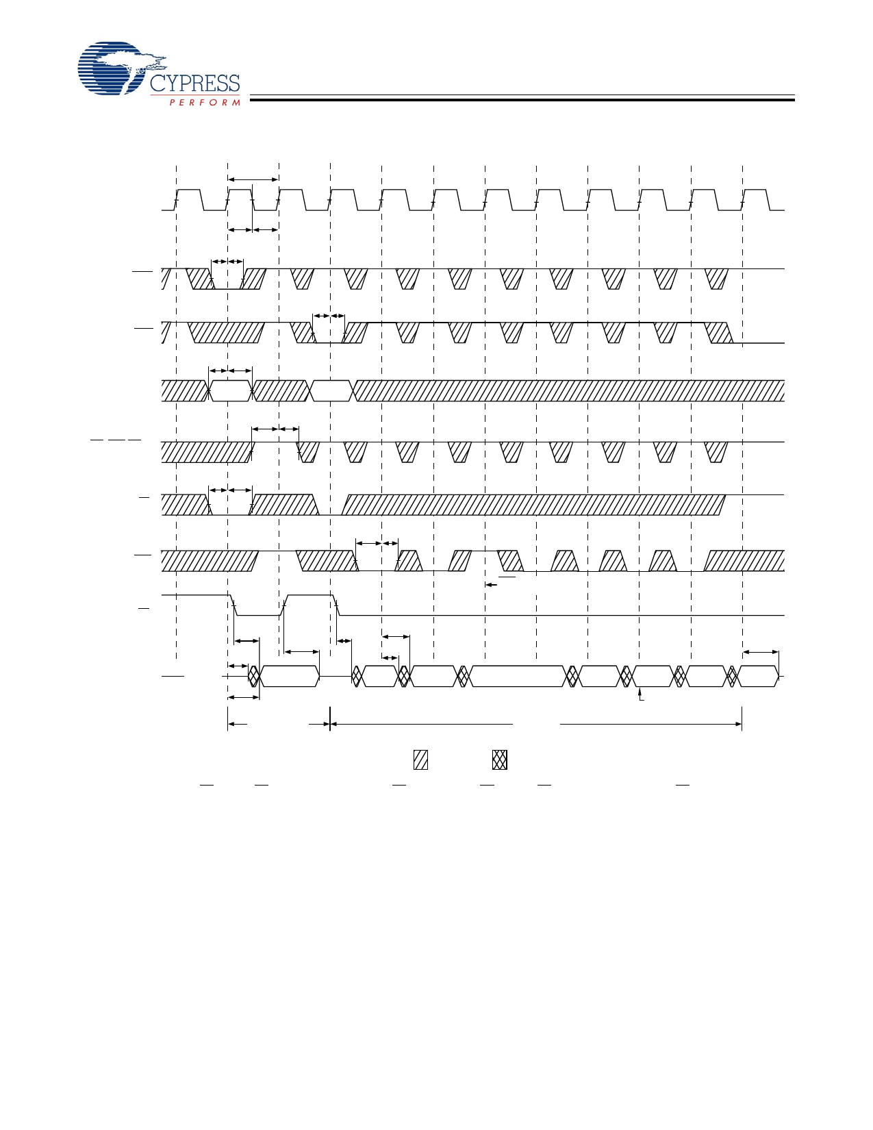
Timing Diagrams
Read Cycle Timing[16]
tCYC
CLK
ADSP
ADSC
t CH t CL
tADS tADH
tADS tADH
tAS tAH
ADDRESS
GW, BWE,BW
[A:B]
CE
ADV
A1
A2
t WES tWEH
tCES tCEH
t
ADVS
tADVH
ADV suspends burst
Deselect Cycle
OE
Data Out (Q)
tOEV
High-Z
tCLZ
tCDV
tOEHZ
Q(A1)
Single READ
tOELZ
tCDV
tDOH
Q(A2) Q(A2 + 1)
Q(A2 + 2)
BURST
READ
Q(A2 + 3)
Q(A2) Q(A2 + 1)
Burst wraps around
to its initial state
tCHZ
Q(A2 + 2)
DON’T CARE UNDEFINED
Note:
16. On this diagram, when CE is LOW: CE1 is LOW, CE2 is HIGH and CE3 is LOW. When CE is HIGH: CE1 is HIGH or CE2 is LOW or CE3 is HIGH.
Document #: 38-05518 Rev. *D
Page 10 of 16
Share Link: 