CY7C1041D View Datasheet(PDF) - Cypress Semiconductor
Part Name
Description
MFG CO.
CY7C1041D Datasheet PDF : 9 Pages
| |||
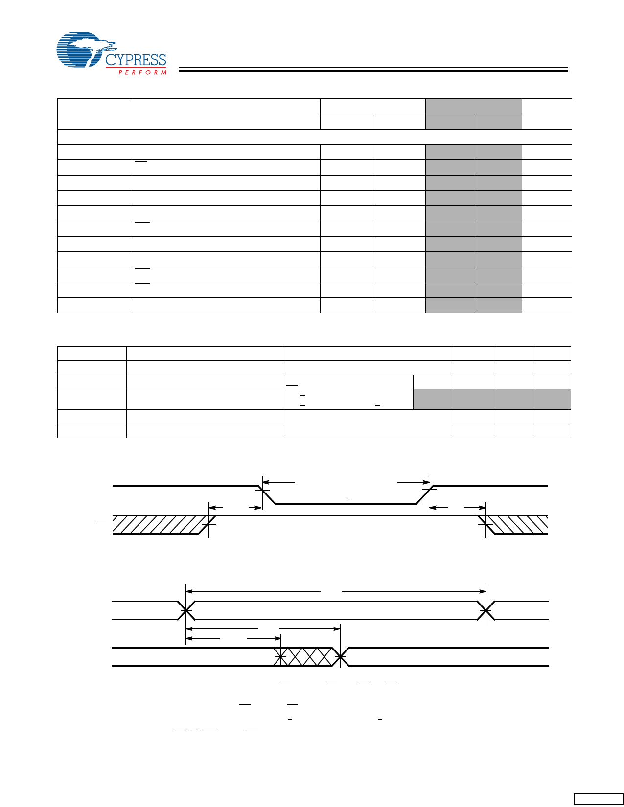
Switching Characteristics[6] Over the Operating Range(continued)
Parameter
Write Cycle[10, 11]
Description
tWC
tSCE
tAW
tHA
tSA
tPWE
tSD
tHD
tLZWE
tHZWE
tBW
Write Cycle Time
CE LOW to Write End
Address Set-Up to Write End
Address Hold from Write End
Address Set-Up to Write Start
WE Pulse Width
Data Set-Up to Write End
Data Hold from Write End
WE HIGH to Low Z[9]
WE LOW to High Z[8, 9]
Byte Enable to End of Write
-10 (Industrial)
Min.
Max.
10
7
7
0
0
7
6
0
3
5
7
CY7C1041D
-12 (Automotive)
Min.
Max.
Unit
12
ns
10
ns
10
ns
0
ns
0
ns
10
ns
7
ns
0
ns
3
ns
6
ns
10
ns
Data Retention Characteristics Over the Operating Range
Parameter
Description
Conditions[13]
VDR
ICCDR
ICCDR
tCDR[4]
tR[12]
VCC for Data Retention
Data Retention Current
Data Retention Current
VCC = VDR = 2.0V,
CE > VCC – 0.3V,
VIN > VCC – 0.3V or VIN < 0.3V
Chip Deselect to Data Retention Time
Operation Recovery Time
Data Retention Waveform
Ind’l
Auto
Min.
2.0
0
tRC
Max. Unit
V
10
mA
15
mA
ns
ns
DATA RETENTION MODE
VCC
4.5V
VDR > 2V
4.5V
tCDR
tR
CE
Switching Waveforms
Read Cycle No. 1[13, 14]
tRC
ADDRESS
DATA OUT
tAA
tOHA
PREVIOUS DATA VALID
DATA VALID
Notes:
10. The internal Write time of the memory is defined by the overlap of CE LOW, and WE LOW. CE and WE must be LOW to initiate a Write, and the transition of
either of these signals can terminate the Write. The input data set-up and hold timing should be referenced to the leading edge of the signal that terminates the
Write.
11. The minimum Write cycle time for Write Cycle No. 3 (WE controlled, OE LOW) is the sum of tHZWE and tSD.
12. Full device operation requires linear VCC ramp from VDR to VCC(min.) > 50 µs or stable at VCC(min.) > 50 µs
13. No input may exceed VCC + 0.5V
14. Device is continuously selected. OE, CE, BHE, and/or BHE = VIL.
Document #: 38-05472 Rev. *C
Page 4 of 9
[+] Feedback
Share Link: 