BD8312HFN(2009) View Datasheet(PDF) - ROHM Semiconductor
Part Name
Description
MFG CO.
BD8312HFN
(Rev.:2009)
(Rev.:2009)
ROHM Semiconductor
BD8312HFN Datasheet PDF : 15 Pages
| |||
BD8312HFN
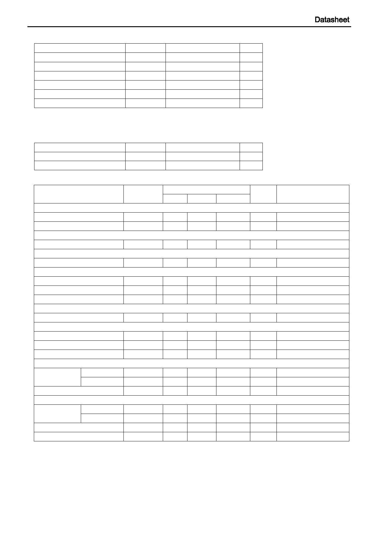
Technical Note
Description of Blocks
1. Reference
This block produces ERROR AMP standard voltage.
The standard voltage is 1.0 V.
2. 5 V Reg
5 V low saturation regulator for internal analog circuit
This IC is equipped with this regulator for the purpose of protecting the internal circuit from voltage.
output is reduced when VCC is less than 5 V, but there is no problem in use.
Therefore, this
3 UVLOT
Circuit for preventing low voltage malfunction
Prevents malfunction of the internal circuit at activation of the power supply voltage or at low power supply voltage.
Monitors VCC pin voltage to turn off all output FET and DC/DC converter output when VCC voltage is lower than 2.9 V,
and reset the timer latch of the internal SCP circuit and soft-start circuit. This threshold contains 200 mV hysteresis.
4 SCP
Timer latch system short-circuit protection circuit
When the INV pin is the set 1.0 V or lower voltage, the internal SCP circuit starts counting.
The internal counter is in synch with OSC; the latch circuit activates about 2.7msec after the counter counts about 4000
oscillations to turn off DC/DC converter output.
To reset the latch circuit, turn off the STB pin once. Then, turn it on again or turn on the power supply voltage again.
5 OSC
Circuit for oscillating sawtooth waves with an operation frequency fixed at 1.5 MHz
6 ERROR AMP
Error amplifier for detecting output signals and output PWM control signals
The internal standard voltage is set at 1.0 V.
A primary phase compensation device of 200 pF, 62 kΩ is built in-between the inverting input terminal and the output
terminal of this ERROR AMP.
7 PWM COMP
Voltage-pulse width converter for controlling output voltage corresponding to input voltage
Comparing the internal SLOPE waveform with the ERROR AMP output voltage, PWM COMP
controls the pulse width to the output to the driver.
8 SOFT START
Circuit for preventing in-rush current at startup by bringing the output voltage of the DC/DC converter into a soft-start
Soft-start time is in synch with the internal OSC, and the output voltage of the DC/DC converter reaches the set voltage
after about 8000 oscillations.
9 PRE DRIVER/TIMING CONTROL
CMOS inverter circuit for driving the built-in synchronous rectification SW
The synchronous rectification OFF time for preventing feedthrough is about 25 nsec.
10 STBY_IO
Voltage applied on STB pin (7 pin) to control ON/OFF of IC
Turned ON when a voltage of 2.5 V or higher is applied and turned OFF when the terminal is open or 0 V is applied.
Incorporates approximately 400 kΩ pull-down resistance.
11 Pch/Nch FET SW
Built-in synchronous rectification SW for switching the coil current of the DC/DC converter
Incorporates a 450 mΩ PchFET SW capable of withstanding 15 V.and 300 mΩ SW capable of withstanding 15 V.
Since the current rating of this FET is 1.0A, it should be used within 1.0A including the DC current and ripple current of the coil.
www.rohm.com
© 2009 ROHM Co., Ltd. All rights reserved.
4/14
2009.04- Rev.B
Share Link: 