BA4510XXX View Datasheet(PDF) - ROHM Semiconductor
Part Name
Description
MFG CO.
BA4510XXX Datasheet PDF : 22 Pages
| |||
BA4510xxx
Datasheet
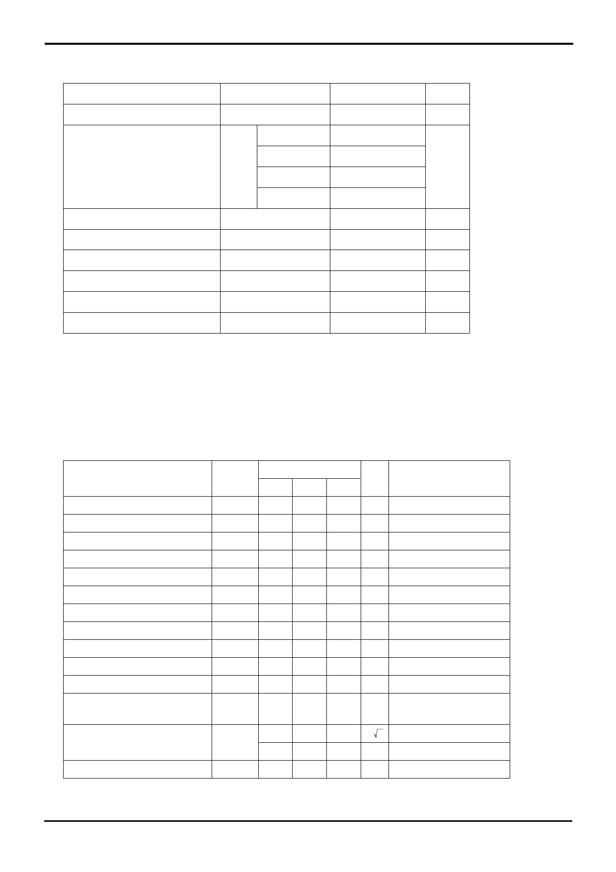
●Absolute Maximum Ratings (Ta=25℃)
○BA4510
Parameter
Symbol
Ratings
Unit
Supply Voltage
Power dissipation
Differential Input Voltage *6
VCC-VEE
SOP8
SSOP-B8
Pd
TSSOP-B8
MSOP8
Vid
+10
620*1*5
550*2*5
500*3*5
470*4*5
VCC-VEE
V
mW
V
Input Common-mode Voltage Range
Vicm
VEE to VCC
V
Operating Supply Voltage
Vopr
2 to 7(±1 to ±3.5)
V
Operating Temperature
Topr
-20 to +75
℃
Storage Temperature
Tstg
-40 to 125
℃
Maximum Junction Temperature
Tjmax
+125
℃
Note: Absolute maximum rating item indicates the condition which must not be exceeded.
Application of voltage in excess of absolute maximum rating or use out absolute maximum rated temperature environment may cause
deterioration of characteristics.
*1 To use at temperature above Ta=25℃ reduce 6.2mW/℃
*2 To use at temperature above Ta=25℃ reduce 5.5mW/℃
*3 To use at temperature above Ta=25℃ reduce 5.0mW/℃
*4 To use at temperature above Ta=25℃ reduce 4.8mW/℃
*5 Mounted on a FR4 glass epoxy PCB(70mm×70mm×1.6mm).
*6 The voltage difference between inverting input and non-inverting input is the differential input voltage.
Then input terminal voltage is set to more than VEE.
●Electrical Characteristics
○BA4510 (Unless otherwise specified VCC=+2.5V, VEE=-2.5V, Ta=25℃)
Parameter
Symbol
Limits
Unit
Min. Typ. Max.
Input Offset Voltage *7
Vio
-
1
6 mV
Input Offset Current *7
Iio
-
2
200 nA
Input Bias Current *8
Ib
-
80 500 nA
Condition
RS=50Ω
-
-
Supply Current
Maximum Output Voltage(High)
Maximum Output Voltage(Low)
ICC
VOH
VOL
2.5 5.0 7.5 mA RL=∞, All Op-Amps
+2.0 +2.4 -
V RL=10kΩ
-
-2.4 -2.0 V RL=10kΩ
Large Signal Voltage Gain
Av
60 90
-
dB RL≧10kΩ
Input Common-mode Voltage Range Vicm -1.3
-
+1.5 V
-
Common-mode Rejection Ratio
CMRR 60 80
- dB
-
Power Supply Rejection Ratio
PSRR 60 80
-
dB RS=50Ω
Slew Rate
SR
-
5.0
- V/μs Av=1
Total Harmonic Distortion+ Noise THD+N - 0.007 -
Av=20dB, RL=10kΩ,
% VIN=0.05Vrms, f=1kHz
DIN-AUDIO
Input Referred Noise Voltage
-
6
- nV/ Hz RS=100Ω, Vi=0V, f=1kHz
Vn
-
0.7
- μVrms DIN-AUDIO
Channel Separation
CS
-
-
dB R1=100Ω, f=1kHz
*7 Absolute value
*8 Current direction: Since first input stage is composed with PNP transistor, input bias current flows out of IC.
www.rohm.com
© 2012 ROHM Co., Ltd. All rights reserved.
TSZ22111・15・00
3/19
TSZ02201-0RAR1G200080-1-2
7.NOV.2012 Rev.001
Share Link: 