BA3474R View Datasheet(PDF) - ROHM Semiconductor
Part Name
Description
MFG CO.
BA3474R Datasheet PDF : 32 Pages
| |||
BA3472xxx, BA3472RFVM, BA3474xxx, BA3474RFV
Datasheet
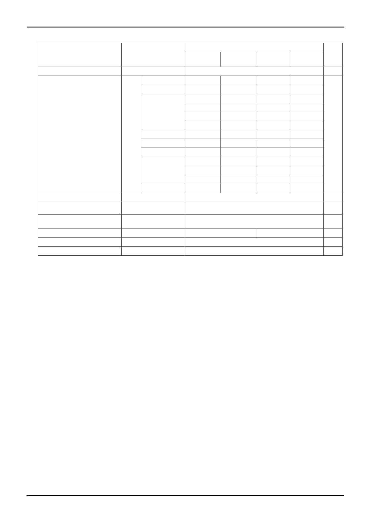
●Absolute Maximum Ratings (Ta=25℃)
Parameter
Symbol
BA3472
Ratings
BA3474 BA3472R
BA3474R
Supply Voltage
Power dissipation
Differential Input Voltage*17
Input Common-mode
Voltage Range
Operable with low voltage
VCC-VEE
SOP8
SSOP-B8
MSOP8
Pd
SOP-J8
TSSOP-B8
SOP14
SSOP-B14
TSSOP-B14
Vid
Vicm
Vopr
780*1*13
690*2*13
590*3*13
-
-
-
675*7*13
625*4*13
-
-
-
-
-
+36
-
-
-
-
-
590*3*13
-
625*4*14
-
713*5*15
-
937*6*16
-
-
-
-
610*8*13
-
870*9*13
-
-
-
-
-
850*12*13
-
+36
(VEE - 0.3) to VEE + 36
+3.0V to +36.0V
(±1.5V to ±18.0V)
-
-
-
-
-
-
-
-
-
870*9*13
1187*10*15
1689*11*16
-
Operating Temperature Range
Topr
-40 to +85(SOP14:to +75)
-40 to +105
Storage Temperature Range
Tstg
-55 to +150
Maximum Junction Temperature
Tjmax
+150
Note: Absolute maximum rating item indicates the condition which must not be exceeded.
Application if voltage in excess of absolute maximum rating or use out of absolute maximum rated temperature environment may cause
deterioration of characteristics.
*1 To use at temperature above Ta=25℃ reduce 6.2mW/℃.
*2 To use at temperature above Ta=25℃ reduce 5.5mW/℃
*3 To use at temperature above Ta=25℃ reduce 4.8mW/℃
*4 To use at temperature above Ta=25℃ reduce 5.0mW/℃
*5 To use at temperature above Ta=25℃ reduce 5.7mW/℃
*6 To use at temperature above Ta=25℃ reduce 7.5mW/℃
*7 To use at temperature above Ta=25℃ reduce 5.4mW/℃
*8 To use at temperature above Ta=25℃ reduce 4.9mW/℃
*9 To use at temperature above Ta=25℃ reduce 7.0mW/℃
*10 To use at temperature above Ta=25℃ reduce 9.5mW/℃
*11 To use at temperature above Ta=25℃ reduce 13.5mW/℃
*12 To use at temperature above Ta=25℃ reduce 6.8mW/℃
*13 Mounted on a FR4 glass epoxy PCB(70mm×70mm×1.6mm).
*14 Mounted on a FR4 glass epoxy 2 layers PCB 70mm×70mm×1.6mm (occupied copper area:15mm×15mm).
*15 Mounted on a FR4 glass epoxy 2 layers PCB 70mm×70mm×1.6mm (occupied copper area:70mm×70mm).
*16 Mounted on a FR4 glass epoxy 4 layers PCB 70mm×70mm×1.6mm (occupied copper area:70mm×70mm).
*17 The voltage difference between inverting input and non-inverting input is the differential input voltage.
Then input terminal voltage is set to more than VEE.
Unit
V
mW
V
V
V
℃
℃
℃
www.rohm.com
© 2012 ROHM Co., Ltd. All rights reserved.
TSZ22111・15・001
4/29
TSZ02201-0RAR0G200100-1-2
26.OCT.2012 Rev.002
Share Link: 