AS7C513B-20TC View Datasheet(PDF) - Alliance Semiconductor
Part Name
Description
MFG CO.
AS7C513B-20TC Datasheet PDF : 9 Pages
| |||
AS7C513B
®
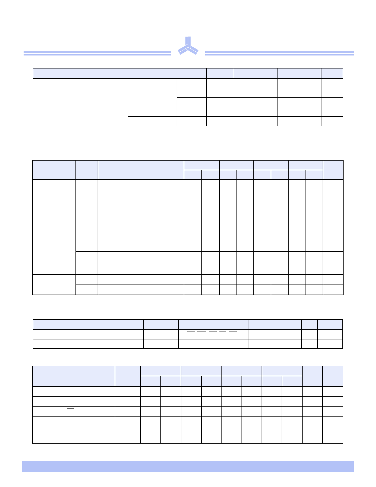
Recommended operating conditions
Parameter
Supply voltage
Input voltage
Ambient operating temperature
commercial
industrial
VIL min = -1.0V for pulse width less than 5ns
VIH max = VCC+2.0V for pulse width less than 5ns.
Symbol
VCC
VIH
VIL
TA
TA
Min
4.5
2.2
–0.5
0
–40
Typical
5
–
–
–
–
Max
5.5
VCC + 0.5
0.8
70
85
Unit
V
V
°C
°C
DC operating characteristics (over the operating range)1
-10
-12
-15
-20
Parameter
Sym
Test conditions
Min Max Min Max Min Max Min Max Unit
Input leakage
current
| ILI |
Output leakage
current
| ILO |
Operating
power supply ICC
current
VCC = Max
VIN = GND to VCC
VCC = Max
VOUT = GND to VCC
VCC = Max, CE ≤ VIL
f = fMax , IOUT = 0mA
– 1 – 1 – 1 – 1 µA
– 1 – 1 – 1 – 1 µA
– 110 – 100 – 90 – 80 mA
ISB
Standby power
supply current
ISB1
Output voltage VOL
VOH
VCC = Max, CE ≥ VIH
f = fMax
VCC = Max, CE ≥ VCC - 0.2V
VIN ≤ 0.2V or
VIN ≥ VCC –0.2V, f = 0
IOL = 8 mA, VCC = Min
IOH = –4 mA, VCC = Min
– 50 – 45 – 45 – 40 mA
– 10 – 10 – 10 – 10 mA
– 0.4 – 0.4 – 0.4 – 0.4 V
2.4 – 2.4 – 2.4 – 2.4 – V
Capacitance (f = 1MHz, Ta = 25o C, VCC = NOMINAL)2
Parameter
Symbol
Signals
Input capacitance
I/O capacitance
CIN
CI/O
A, CE, WE, OE, LB, UB
I/O
Test conditions
Vin = 0V
Vin = Vout = 0V
Max Unit
5 pF
7 pF
Read cycle (over the operating range) 3,9
-10
Parameter
Symbol Min Max
Read cycle time
tRC
10
–
Address access time
tAA
– 10
Chip enable (CE) access time
tACE
–
10
Output enable (OE) access time tOE
–
5
Output hold from address
change
tOH
3
–
-12
Min Max
12
–
–
12
–
12
–
6
3
–
-15
Min Max
15 –
– 15
– 15
–
7
3
–
-20
Min Max
20 –
– 20
– 20
–
8
3
–
Unit Notes
ns
ns
3
ns
3
ns
ns
5
3/26/04, v.1.3
Alliance Semiconductor
P. 3 of 9
Share Link: 