APL3218 View Datasheet(PDF) - Anpec Electronics
Part Name
Description
MFG CO.
APL3218 Datasheet PDF : 20 Pages
| |||
APL3218
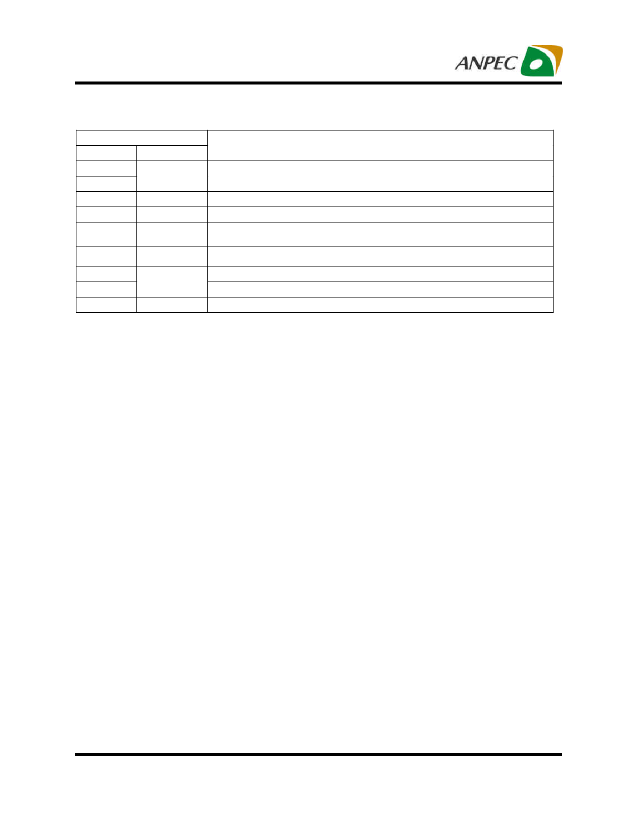
Pin Description
PIN
NO
NAME
1
ACIN
2
3
GND
4
VCDT
5
GATDRV
6
7
8
Exposed Pad
CHR_LDO
OUT
-
FUNCTION
Power Supply Input. Connect this pin to external DC supply. Bypass to GND with a 1µF
(minimum) ceramic capacitor.
Ground terminal.
Provide an interval voltage divider. This pin divides ACIN voltage into 39/369 ratio.
Charging current control pin. When sourcing a current from this pin, the OUT pin will source
out a current whose magnitude is 200xIGATDRV .
Output Pin. The pin provides supply voltage to the PMIC input. Bypass to GND with a 1µF
(minimum) ceramic capacitor.
Output Pins. The pin provides supply source current in series with a resistor to battery.
This pin possesses the overshoot clamp function to limit peak voltage.
Exposed Thermal Pad. Must be electrically connected to the GND pin.
Copyright © ANPEC Electronics Corp.
9
Rev. A.1 - Apr., 2012
www.anpec.com.tw
Share Link: 