AN-90 View Datasheet(PDF) - Fairchild Semiconductor
Part Name
Description
MFG CO.
AN-90 Datasheet PDF : 7 Pages
| |||
AN006021-6
FIGURE 4. Guaranteed Noise Margin
over Temperature vs VCC
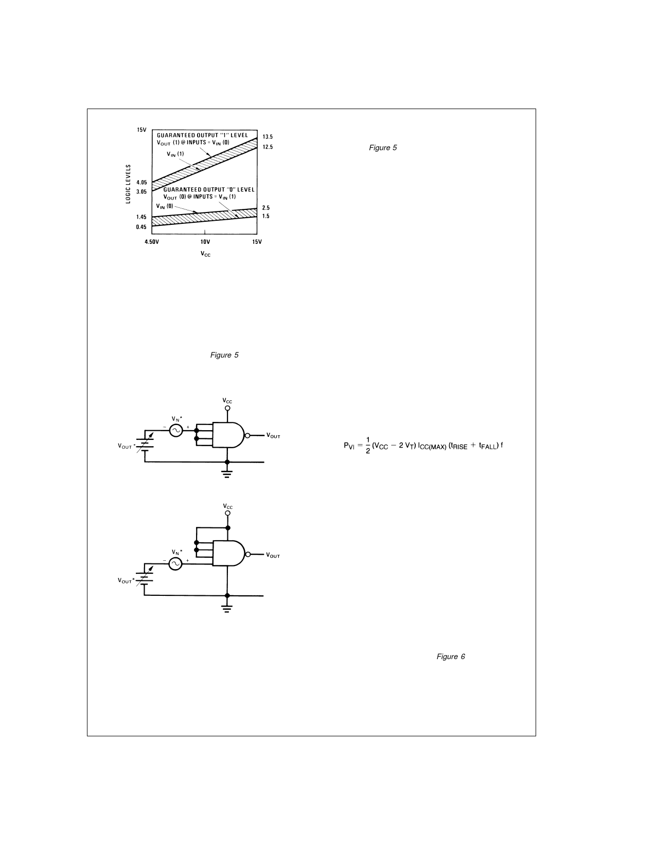
Noise immunity is an important device characteristic. How-
ever, noise margin is of more use to the designer because it
very simply defines the amount of noise a system can toler-
ate under any circumstances and still maintain the integrity
of logic levels.
Any noise specification to be complete must define how
measurements are to be made. Figure 5 indicates two ex-
treme cases; driving all inputs simultaneously and driving
one input at a time. Both conditions must be included be-
cause each represents one worst case extreme.
this guarantees that every node within a system can have
1.0V of noise, in logic “1” or logic “0” state, without malfunc-
tioning. This could not be guaranteed without testing for both
conditions in Figure 5.
POWER CONSUMPTION
There are four sources of power consumption in CMOS de-
vices: (1) leakage current; (2) transient power due to load ca-
pacitance; (3) transient power due to internal capacitance
and; (4) transient power due to current spiking during switch-
ing.
The first, leakage current, is the easiest to calculate and is
simply the leakage current times VCC. The data sheet for
each specific device specifies this leakage current.
The second, transient power due to load capacitance, can
be derived from the fact that the energy stored on a capacitor
is 1/2 CV2. Therefore every time the load capacitance is
charged or discharged this amount of energy must be pro-
vided by the CMOS device. The energy per cycle is then
2[(1/2) CVCC2] = CVCC2. Energy per unit time, or power, is
then CVCC2 f, where C is the load capacitance and f is the
frequency.
The third, transient power due to internal capacitance takes
exactly the same form as the load capacitance. Every device
has some internal nodal capacitance which must be charged
and discharged. This then represents another power term
which must be considered.
The fourth, transient power due to switching current, is
caused by the fact that whenever a CMOS device goes
through a transition, with VCC ≥ 2 VT, there is a time when
both N-channel and P-channel devices are both conducting.
An expression for this current is derived in Application Note
AN-77. The expression is:
(A)
AN006021-7
*VOUT = VOUT (1) MIN, VOUT (0) MAX
VN = Allowable Noise Voltage = 1.0V
(B)
AN006021-8
FIGURE 5. Noise Margin Test Circuits
To guarantee a noise margin of 1.0V, all 54C/74C devices
are tested under both conditions. It is important to note that
where:
VT = threshold voltage
ICC(MAX) = peak non-capacitive current during switching
f = frequency
Note that this expression, like the capacitive power term is
directly proportional to frequency. If the PVI term is combined
with the term arising from the internal capacitance, a capaci-
tance CPD may be defined which closely approximates the
no load power consumption for a CMOS device when used
in the following expression:
Power (no load) = CPD VCC2 f
The total power consumption is then simplified to:
Total Power = (CPD + CL) VCC2 f + ILEAK VCC(1)
The procedure for obtaining CPD is to measure the no load
power at VCC = 10V vs frequency and calculate the value of
CPD which corresponds to the measured power consump-
tion. This value of CPD is given on each 54C/74C data sheet
and with equation (1) the computation of power consumption
is straightforward.
To simplify the task even further Figure 6 gives a graph of
normalized power vs frequency for different power supply
3
www.fairchildsemi.com
Share Link: 