EDS1232CATA View Datasheet(PDF) - Elpida Memory, Inc
Part Name
Description
MFG CO.
EDS1232CATA Datasheet PDF : 55 Pages
| |||
EDS1232CABB, EDS1232CATA
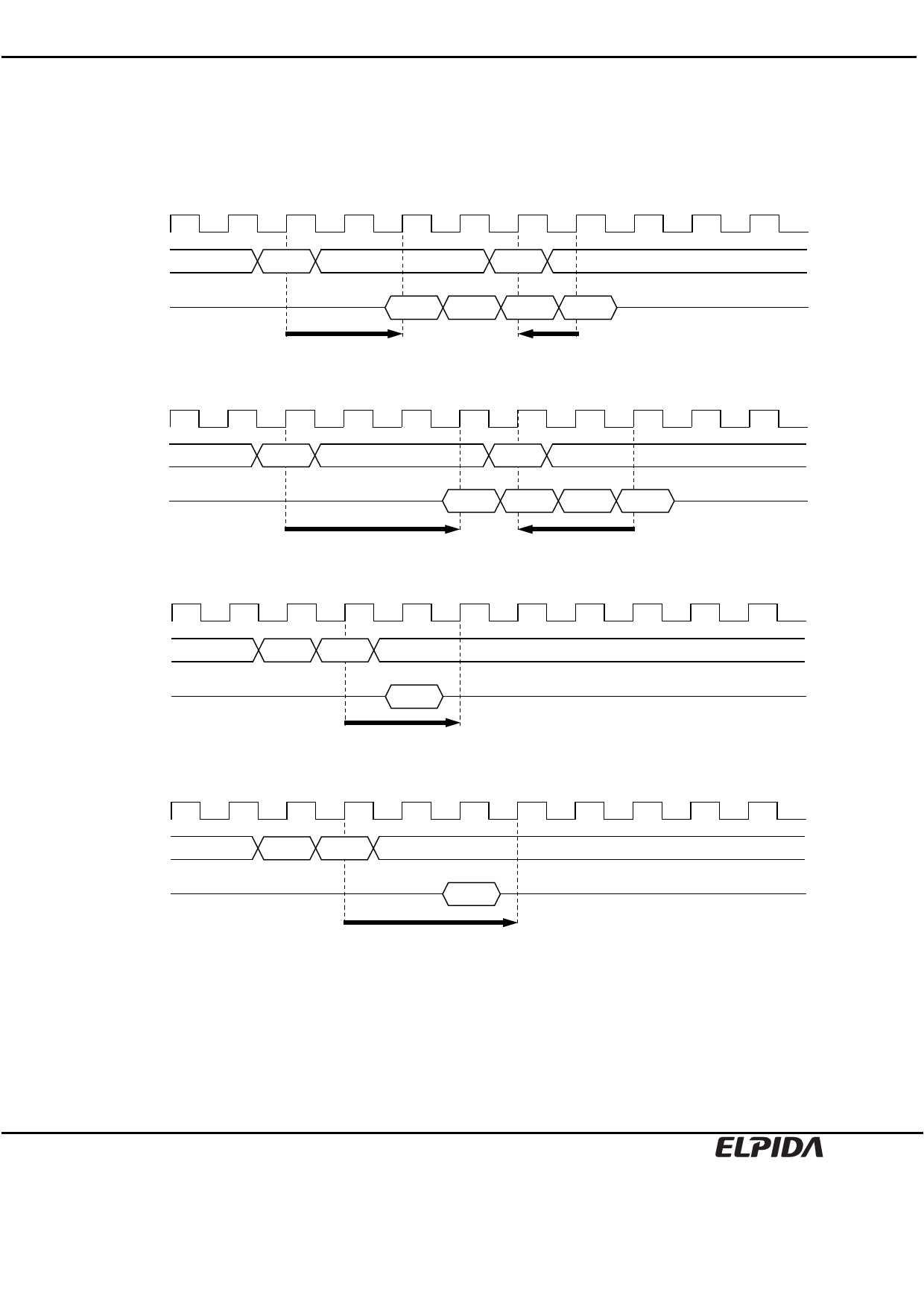
Read command to Precharge command interval (same bank)
When the precharge command is executed for the same bank as the read command that preceded it, the minimum
interval between the two commands is one clock. However, since the output buffer then becomes High-Z after the
clocks defined by lHZP, there is a case of interruption to burst read data output will be interrupted, if the precharge
command is input during burst read. To read all data by burst read, the clocks defined by lEP must be assured as
an interval from the final data output to precharge command execution.
CLK
Command
READ
PRE/PALL
DQ
out A0
out A1
out A2
out A3
CL=2
lEP = -1 cycle
READ to PRECHARGE Command Interval (same bank): To output all data (CL = 2, BL = 4)
CLK
Command
READ
PRE/PALL
DQ
out A0
out A1
out A2
out A3
CL=3
lEP = -2 cycle
READ to PRECHARGE Command Interval (same bank): To output all data (CL = 3, BL = 4)
CLK
Command
DQ
READ PRE/PALL
out A0
High-Z
lHZP = 2
READ to PRECHARGE Command Interval (same bank): To stop output data (CL = 2, BL = 1, 2, 4, 8)
CLK
Command
READ PRE/PALL
High-Z
DQ
out A0
lHZP =3
READ to PRECHARGE Command Interval (same bank): To stop output data (CL = 3, BL = 1, 2, 4, 8)
Preliminary Data Sheet E0247E40 (Ver. 4.0)
39
Share Link: 