ADT7483AARQZ View Datasheet(PDF) - ON Semiconductor
Part Name
Description
MFG CO.
ADT7483AARQZ Datasheet PDF : 24 Pages
| |||
ADT7483A
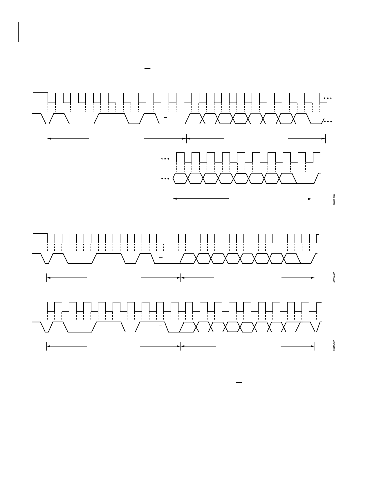
write operation contains a second data byte that is written to the
register selected by the address pointer register (see Figure 16).
The device address is sent over the bus followed by R/W set
to 0. This is followed by two data bytes. The first data byte is
1
SCL
the address of the internal data register to be written to, which
is stored in the address pointer register. The second data byte is
the data to be written to the internal data register.
9
1
9
SDA
1
0
START BY
MASTER
0
1
1
0
1
R/W
D7
D6
D5
D4
D3
D2
D1
D0
FRAME 1
SERIAL BUS ADDRESS BYTE
ACK. BY
ADT7483A
FRAME 2
ADDRESS POINTER REGISTER BYTE
ACK. BY
ADT7483A
1
9
SCL (CONTINUED)
SDA (CONTINUED)
D7
D6
D5
D4
D3
D2
D1
D0
FRAME 3
DATA
BYTE
ACK. BY
ADT7483A
Figure 16. Writing a Register Address to the Address Pointer Register, then Writing Data to the Selected Register
STOP BY
MASTER
1
9
1
9
SCL
SDA
1
0
START BY
MASTER
1
SCL
0
1
1
0
1
R/W
D7
D6
D5
D4
D3
D2
D1
FRAME 1
SERIAL BUS ADDRESS BYTE
ACK. BY
ADT7483A
FRAME 2
ADDRESS POINTER REGISTER BYTE
Figure 17. Writing to the Address Pointer Register Only
9
1
D0
ACK. BY STOP BY
ADT7483A MASTER
9
SDA
1
0
START BY
MASTER
0
1
1
0
1
R/W
D7
D6
D5
D4
D3
D2
D1
FRAME 1
SERIAL BUS ADDRESS BYTE
ACK. BY
ADT7483A
FRAME 2
DATA BYTE FROM ADT7483A
Figure 18. Reading from a Previously Selected Register
D0
ACK. BY STOP BY
MASTER MASTER
When reading data from a register there are two possibilities:
• If the address pointer register value of the ADT7483A is
unknown or not the desired value, it is first necessary to set
it to the correct value before data can be read from the
desired data register. This is done by performing a write to
the ADT7483A as before, but only the data byte containing
the register read address is sent, as data is not to be written
to the register (see Figure 17).
A read operation is then performed consisting of the serial
bus address, R/W bit set to 1, followed by the data byte
read from the data register (see Figure 18).
• If the address pointer register is known to be already at the
desired address, data can be read from the corresponding
data register without first writing to the address pointer
register and the bus transaction shown in Figure 17 can
be omitted.
Rev. 1 | Page 18 of 24 | www.onsemi.com
Share Link: 