AD8468WBKSZ-RL(Rev0) View Datasheet(PDF) - Analog Devices
Part Name
Description
MFG CO.
AD8468WBKSZ-RL
(Rev.:Rev0)
(Rev.:Rev0)
Analog Devices
AD8468WBKSZ-RL Datasheet PDF : 12 Pages
| |||
AD8468
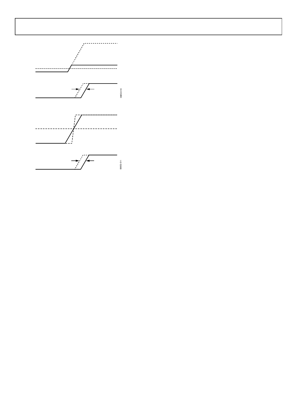
INPUT VOLTAGE
500mV OVERDRIVE
10mV OVERDRIVE
VN ± VOS
DISPERSION
Q OUTPUT
Figure 10. Propagation Delay—Overdrive Dispersion
INPUT VOLTAGE
1V/ns
10V/ns
VN ± VOS
DISPERSION
Q OUTPUT
Figure 11. Propagation Delay—Slew Rate Dispersion
CROSSOVER BIAS POINT
Rail-to-rail inputs of this type, in both op amps and comparators,
have a dual front-end design. Certain devices are active near the
VCC rail and others are active near the VEE rail or ground. At some
predetermined point in the common-mode range, a crossover
occurs. At this point, normally VCC/2, the direction of the bias
current reverses, and there are changes in measured offset
voltages and currents.
The AD8468 slightly elaborates on this scheme. Crossover
points can be found at approximately 0.8 V and 1.6 V.
MINIMUM INPUT SLEW RATE REQUIREMENT
With the rated load capacitance and normal good PC board
design practice, as discussed in the Optimizing Performance
section, these comparators should be stable at any input slew
rate with no hysteresis. Broadband noise from the input stage is
observed in place of the violent chattering seen with most other
high speed comparators. With additional capacitive loading or
poor bypassing, oscillation may be encountered. These oscilla-
tions are due to the high gain bandwidth of the comparator in
combination with feedback through parasitics in the package
and PC board. In many applications, chattering is not harmful.
Rev. 0 | Page 8 of 12
Share Link: 