AD7879ACPZ-RL(Rev0) View Datasheet(PDF) - Analog Devices
Part Name
Description
MFG CO.
AD7879ACPZ-RL Datasheet PDF : 36 Pages
| |||
AD7879
PIN CONFIGURATION AND FUNCTION DESCRIPTIONS
BALL A1
INDICATOR
1
2
3
AUX/
VBAT/
GPIO
VCC/REF
X+
A
PENIRQ/
INT/DAV CS
Y+
B
DOUT DIN X–
C
SCL GND Y–
D
TOP VIEW
(BALL SIDE DOWN)
Not to Scale
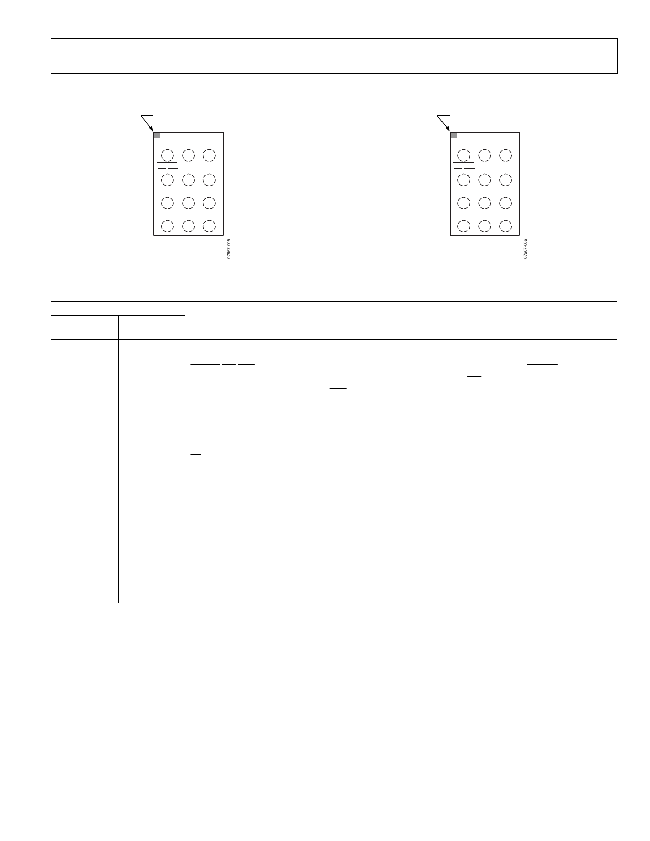
Figure 5. AD7879 WLCSP Pin Configuration
BALL A1
INDICATOR
1
2
3
AUX/
VBAT/
GPIO
VCC/REF
X+
A
PENIRQ/
INT/DAV ADD0 Y+
B
SDA ADD1 X–
C
SCL GND Y–
D
TOP VIEW
(BALL SIDE DOWN)
Not to Scale
Figure 7. AD7879-1 WLCSP Pin Configuration
Y+ 1
NC 2
NC 3
X– 4
PIN 1
INDICATOR
AD7879
TOP VIEW
(Not to Scale)
12 PENIRQ/INT/DAV
11 NC
10 NC
9 DOUT
Y+ 1
NC 2
NC 3
X– 4
PIN 1
INDICATOR
AD7879-1
TOP VIEW
(Not to Scale)
12 PENIRQ/INT/DAV
11 NC
10 NC
9 SDA
NOTES
1. NC = NO CONNECT
2. THE EXPOSED PAD IS NOT CONNECTED INTERNALLY.
FOR INCREASED RELIABILITY OF THE SOLDER JOINTS
AND MAXIMUM THERMAL CAPABILITY IT IS RECOMMENDED
THAT THE PAD BE SOLDERED TO THE GROUND PLANE.
Figure 6. AD7879 LFCSP Pin Configuration
NOTES
1. NC = NO CONNECT
2. THE EXPOSED PAD IS NOT CONNECTED INTERNALLY.
FOR INCREASED RELIABILITY OF THE SOLDER JOINTS
AND MAXIMUM THERMAL CAPABILITY IT IS RECOMMENDED
THAT THE PAD BE SOLDERED TO THE GROUND PLANE.
Figure 8. AD7879-1 LFCSP Pin Configuration
Table 5. Pin Function Descriptions
Pin No.
WLCSP LFCSP
Mnemonic
1A
13
AUX/VBAT/GPIO
1B
12
PENIRQ/INT/DAV
1C
9
1D
8
2A
15
2B
14
2C
6
2D
7
DOUT
SDA
SCL
VCC/REF
CS
ADD0
DIN
ADD1
GND
3A
16
X+
3B
1
Y+
3C
4
X−
3D
5
Y−
N/A
2, 3, 10, 11 NC
N/A
17
EP
Description
Pin functionality is programmable to be either an auxiliary input to the ADC, as a battery measurement
input to the ADC, or as a general-purpose digital input/output.
Interrupt Output. This pin asserts either when the screen is touched, when new data is available in the registers, or
when a measurement exceeds the preprogrammed limits. Active low, internal pull-up resistor of 50 kΩ.
SPI Serial Data Output on the AD7879.
Serial Data Input and Output on the AD7879-1.
Serial Interface Clock Input.
Power Supply Input. It is also the ADC reference.
Chip Select for the Serial Interface on the AD7879. Active low.
Address Bit 0 for the AD7879-1. This pin can be tied high or low to determine an address for the AD7879-1.
SPI Serial Data Input to the AD7879.
Address Bit 1 for the AD7879-1. This pin can be tied high or low to determine an address for the AD7879-1.
Ground. Ground reference point for all circuitry on the AD7879. All analog input signals and any external
reference signal should be referred to this voltage.
Touch Screen Input Channel.
Touch Screen Input Channel.
Touch Screen Input Channel.
Touch Screen Input Channel.
No Connect.
Exposed Pad.
Rev. 0 | Page 7 of 36
Share Link: 