AD7329BRUZ View Datasheet(PDF) - Analog Devices
Part Name
Description
MFG CO.
AD7329BRUZ
Analog Devices
AD7329BRUZ Datasheet PDF : 40 Pages
| |||
AD7329
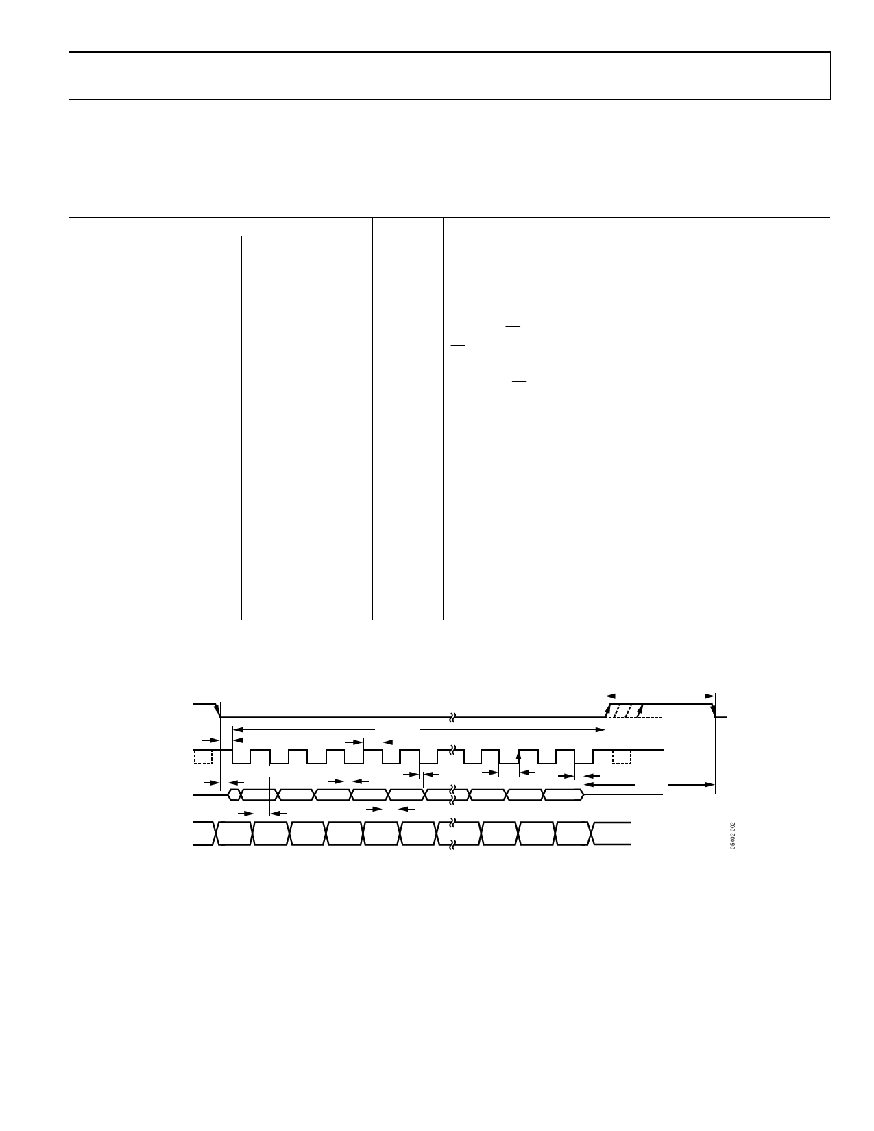
TIMING SPECIFICATIONS
VDD = 12 V to 16.5 V, VSS = −12 V to −16.5 V, VCC = 4.75 V to 5.25 V, VDRIVE = 2.7 V to 5.25 V, VREF = 2.5 V internal/external, TA = TMAX to
TMIN. Timing specifications apply with a 32 pF load, unless otherwise noted. MUXOUT+ is connected directly to ADCIN+ and MUXOUT− is
connected directly to ADCIN−, which is connected to GND for single-ended mode.
Table 3.
Parameter
fSCLK
tCONVERT
tQUIET
t1
t2 1
t3
t4
t5
t6
t7
t8
t9
t10
tPOWER-UP
Limit at TMIN, TMAX
VCC < 4.75 V
VCC = 4.75 V to 5.25 V
50
50
14
20
16 × tSCLK
75
16 × tSCLK
60
12
5
25
20
45
35
26
14
57
43
0.4 × tSCLK
0.4 × tSCLK
13
0.4 × tSCLK
0.4 × tSCLK
8
40
22
10
9
4
4
2
2
750
750
500
500
Unit
kHz min
MHz max
ns max
ns min
ns min
ns min
ns min
ns max
ns max
ns min
ns min
ns min
ns max
ns min
ns min
ns min
ns max
μs max
25
25
μs typ
Description
VDRIVE ≤ VCC
tSCLK = 1/fSCLK
Minimum time between end of serial read and next falling edge of CS
Minimum CS pulse width
CS to SCLK setup time; bipolar input ranges (±10 V, ±5 V, ±2.5 V)
Unipolar input range (0 V to 10 V)
Delay from CS until DOUT three-state disabled
Data access time after SCLK falling edge
SCLK low pulse width
SCLK high pulse width
SCLK to data valid hold time
SCLK falling edge to DOUT high impedance
SCLK falling edge to DOUT high impedance
DIN setup time prior to SCLK falling edge
DIN hold time after SCLK falling edge
Power-up from autostandby
Power-up from full shutdown/autoshutdown mode, internal
reference
Power-up from full shutdown/autoshutdown mode, external
reference
1 When using VCC = 4.75 V to 5.25 V and the 0 V to 10 V unipolar range, running at 1 MSPS throughput rate with t2 at 20 ns, the mark-space ratio must be limited to 50:50.
CS
tCONVERT
t2
t6
SCLK
1
2
3
4
5
3 IDENTIFICATION BITS
t3
DOUT
ADD1 ADD0 SIGN
THREE- ADD2
STATE
t9
t4 t7
DB11 DB10
t10
DIN
WRITE
REG
SEL1
REG
SEL2
MSB
t1
13
14
t5
DB2 DB1
15
DB0
16
t8
tQUIET
THREE-STATE
LSB
0
Figure 2. Serial Interface Timing Diagram
Rev. A | Page 7 of 40
Share Link: 