AD7324 View Datasheet(PDF) - Analog Devices
Part Name
Description
MFG CO.
AD7324 Datasheet PDF : 36 Pages
| |||
AD7324
THEORY OF OPERATION
CIRCUIT INFORMATION
The AD7324 is a fast, 4-channel, 12-bit plus sign, bipolar input,
serial A/D converter. The AD7324 can accept bipolar input ranges
that include ±10 V, ±5 V, and ±2.5 V; it can also accept a 0 V to
+10 V unipolar input range. A different analog input range can
be programmed on each analog input channel via the on-chip
registers. The AD7324 has a high speed serial interface that can
operate at throughput rates up to 1 MSPS.
The AD7324 requires VDD and VSS dual supplies for the high voltage
analog input structures. These supplies must be equal to or greater
than the analog input range. See Table 6 for the requirements of
these supplies for each analog input range. The AD7324 requires
a low voltage 2.7 V to 5.25 V VCC supply to power the ADC core.
Table 6. Reference and Supply Requirements
for Each Analog Input Range
Selected Analog Reference Full-Scale
Input Range (V) Voltage (V) Input Range (V) AVCC (V)
±10
2.5
±10
3/5
3.0
±12
3/5
±5
2.5
±5
3/5
3.0
±6
3/5
±2.5
2.5
±2.5
3/5
3.0
±3
3/5
0 to +10
2.5
0 to +10
3/5
3.0
0 to +12
3/5
Minimum
VDD/VSS (V)
±10
±12
±5
±6
±5
±5
+10/AGND
+12/AGND
To meet the specified performance specifications when the
AD7324 is configured with the minimum VDD and VSS supplies
for a chosen analog input range, the throughput rate should be
decreased from the maximum throughput range (see the
Typical Performance Characteristics section). Figure 18 and
Figure 19 show the change in INL and DNL as the VDD and VSS
voltages are varied. When operating at the maximum throughput
rate, as the VDD and VSS supply voltages are reduced, the INL
and DNL error increases. However, as the throughput rate is
reduced with the minimum VDD and VSS supplies, the INL and
DNL error is reduced.
Figure 31 shows the change in THD as the VDD and VSS supplies
are reduced. At the maximum throughput rate, the THD degrades
significantly as VDD and VSS are reduced. It is therefore necessary
to reduce the throughput rate when using minimum VDD and
VSS supplies so that there is less degradation of THD and the
specified performance can be maintained. The degradation is
due to an increase in the on resistance of the input multiplexer
when the VDD and VSS supplies are reduced.
The analog inputs can be configured as four single-ended
inputs, two true differential input pairs, two pseudo differential
inputs, or three pseudo differential inputs. Selection can be
made by programming the mode bits, Mode 0 and Mode 1, in
the control register.
The serial clock input accesses data from the part and provides
the clock source for the successive approximation ADC. The
AD7324 has an on-chip 2.5 V reference. However, the AD7324
can also work with an external reference. On power-up, the
external reference operation is the default option. If the internal
reference is the preferred option, the user must write to the
reference bit in the control register to select the internal
reference operation.
The AD7324 also features power-down options to allow power
saving between conversions. The power-down modes are
selected by programming the on-chip control register as
described in the Modes of Operation section.
CONVERTER OPERATION
The AD7324 is a successive approximation analog-to-digital
converter built around two capacitive DACs. Figure 23 and
Figure 24 show simplified schematics of the ADC in single-
ended mode during the acquisition and conversion phases,
respectively. Figure 25 and Figure 26 show simplified
schematics of the ADC in differential mode during acquisition
and conversion phases, respectively. The ADC is composed of
control logic, a SAR, and capacitive DACs. In Figure 23 (the
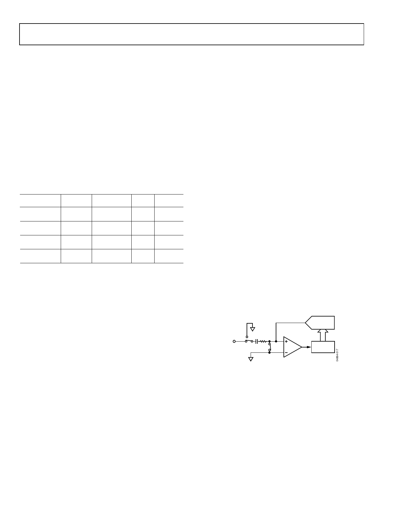
acquisition phase), SW2 is closed and SW1 is in Position A, the
comparator is held in a balanced condition, and the sampling
capacitor array acquires the signal on the input.
VIN0
B
CS
A SW1
CAPACITIVE
DAC
COMPARATOR
SW2
CONTROL
LOGIC
AGND
Figure 23. ADC Acquisition Phase (Single-Ended)
When the ADC starts a conversion (Figure 24), SW2 opens and
SW1 moves to Position B, causing the comparator to become
unbalanced. The control logic and the charge redistribution
DAC are used to add and subtract fixed amounts of charge from
the capacitive DAC to bring the comparator back into a
balanced condition. When the comparator is rebalanced, the
conversion is complete. The control logic generates the ADC
output code.
Rev. 0 | Page 16 of 36
Share Link: 