AD5415(Rev0) View Datasheet(PDF) - Analog Devices
Part Name
Description
MFG CO.
AD5415
(Rev.:Rev0)
(Rev.:Rev0)
Analog Devices
AD5415 Datasheet PDF : 28 Pages
| |||
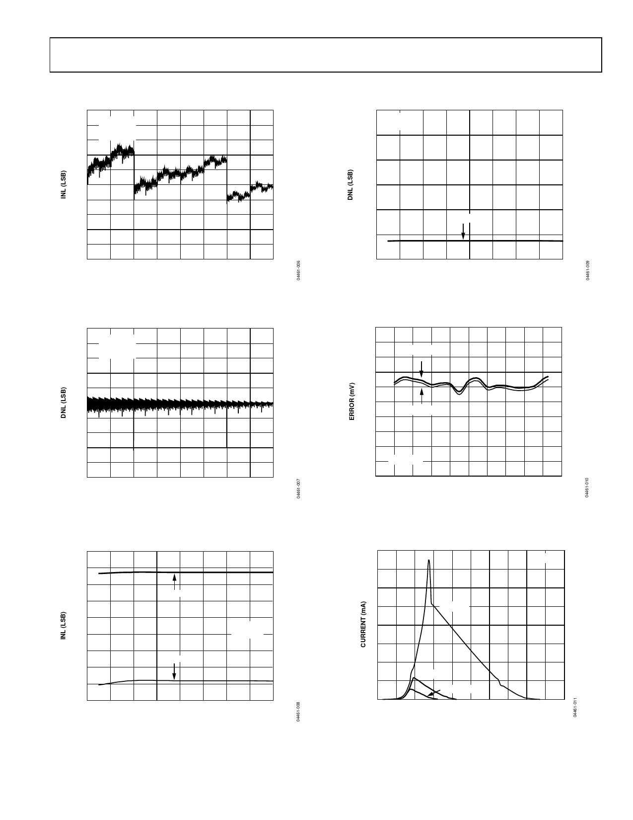
TERMINOLOGY
Relative Accuracy
Relative accuracy or endpoint nonlinearity is a measure of the
maximum deviation from a straight line passing through the
endpoints of the DAC transfer function. It is measured after
adjusting for zero scale and full scale, and is normally expressed
in LSB or as a percentage of full-scale reading.
Differential Nonlinearity
Differential nonlinearity is the difference in the measured
change and the ideal 1 LSB change between any two adjacent
codes. A specified differential nonlinearity of ±1 LSB maximum
over the operating temperature range ensures monotonicity.
Gain Error
Gain error or full-scale error is a measure of the output error
between an ideal DAC and the actual device output. For these
DACs, ideal maximum output is VREF − 1 LSB. Gain error of the
DACs is adjustable to zero with external resistance.
Output Leakage Current
Output leakage current is current that flows in the DAC ladder
switches when they are turned off. For the IOUT1 terminal, it can
be measured by loading all 0s to the DAC and measuring the
IOUT1 current. Minimum current flows in the IOUT2 line when
the DAC is loaded with all 1s.
Output Capacitance
Capacitance from IOUT1 or IOUT2 to AGND.
Output Current Settling Time
The amount of time it takes for the output to settle to a speci-
fied level for a full-scale input change. For these devices, it is
specified with a 100 Ω resistor to ground.
Digital-to-Analog Glitch Impulse
The amount of charge injected from the digital inputs to the
analog output when the inputs change state. This is normally
specified as the area of the glitch in either pA-s or nV-s depend-
ing upon whether the glitch is measured as a current or
voltage signal.
Digital Feedthrough
When the device is not selected, high frequency logic activity on
the device’s digital inputs is capacitively coupled through the
device to show up as noise on the IOUT pins and subsequently
into the following circuitry. This noise is digital feedthrough.
Multiplying Feedthrough Error
The error due to capacitive feedthrough from the DAC
reference input to the DAC IOUT1 terminal when all 0s are
loaded to the DAC.
AD5415
Digital Crosstalk
The glitch impulse transferred to the outputs of one DAC in
response to a full-scale code change (all 0s to all 1s and vice
versa) in the input register of the other DAC. It is expressed
in nV-s.
Analog Crosstalk
The glitch impulse transferred to the output of one DAC due to
a change in the output of another DAC. It is measured by
loading one of the input registers with a full-scale code change
(all 0s to all 1s and vice versa), while keeping LDAC high. Then
pulse LDAC low and monitor the output of the DAC whose
digital code was not changed. The area of the glitch is expressed
in nV-s.
Channel-to-Channel Isolation
The proportion of input signal from one DAC reference input
that appears at the output of the other DAC and is expressed
in dB.
Harmonic Distortion
The DAC is driven by an ac reference. The ratio of the rms sum
of the harmonics of the DAC output to the fundamental value is
the total harmonic distortion (THD). Usually only the lower-
order harmonics are included, such as second to fifth.
( ) THD = 20 log V22 + V32 + V42 + V52
V1
Intermodulation Distortion
The DAC is driven by two combined sine wave references of
frequencies fa and fb. Distortion products are produced at sum
and difference frequencies of mfa ± nfb, where m, n = 0, 1, 2, 3 ...
Intermodulation terms are those for which m or n is not equal
to zero. The second-order terms include (fa + fb) and (fa − fb)
and the third-order terms are (2fa + fb), (2fa − fb), (f + 2fa +
2fb) and (fa − 2fb). IMD is defined as
( ) IMD = 20log rms sumof the sumand diff distortion products
rmsamplitudeof the fundamental
Compliance Voltage Range
The maximum range of (output) terminal voltage for which the
device provides the specified characteristics.
Rev. 0 | Page 9 of 28
Share Link: 