AD5161(Rev0) View Datasheet(PDF) - Analog Devices
Part Name
Description
MFG CO.
AD5161 Datasheet PDF : 20 Pages
| |||
AD5161
TIMING CHARACTERISTICS—5 kΩ, 10 kΩ, 50 kΩ, 100 kΩ VERSIONS
(VDD = +5V ± 10%, or +3V ± 10%; VA = VDD; VB = 0 V; –40°C < TA < +125°C; unless otherwise noted.)
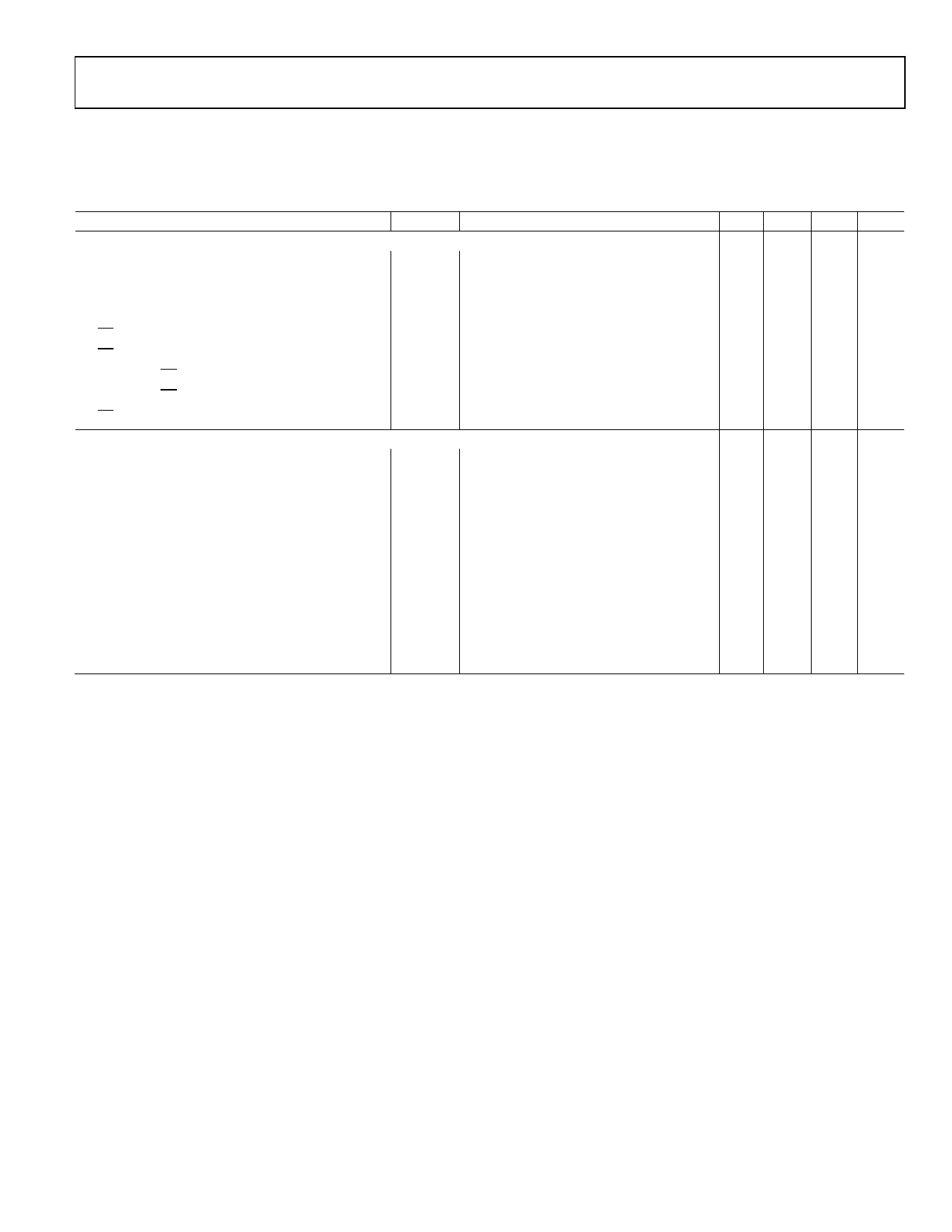
Table 3.
Parameter
Symbol Conditions
SPI INTERFACE TIMING CHARACTERISTICS6, 10 (Specifications Apply to All Parts)
Clock Frequency
fCLK
Input Clock Pulsewidth
tCH, tCL
Clock level high or low
Data Setup Time
tDS
Data Hold Time
tDH
CS Setup Time
tCSS
CS High Pulsewidth
tCSW
CLK Fall to CS Fall Hold Time
tCSH0
CLK Fall to CS Rise Hold Time
tCSH1
CS Rise to Clock Rise Setup
tCS1
I2C INTERFACE TIMING CHARACTERISTICS6, 11 (Specifications Apply to All Parts)
SCL Clock Frequency
fSCL
tBUF Bus Free Time between STOP and START
t1
tHD;STA Hold Time (Repeated START)
t2
After this period, the first clock pulse is
generated.
tLOW Low Period of SCL Clock
t3
tHIGH High Period of SCL Clock
t4
tSU;STA Setup Time for Repeated START Condition t5
tHD;DAT Data Hold Time
t6
tSU;DAT Data Setup Time
t7
tF Fall Time of Both SDA and SCL Signals
t8
tR Rise Time of Both SDA and SCL Signals
t9
tSU;STO Setup Time for STOP Condition
t10
Min Typ1 Max Unit
25 MHz
20
ns
5
ns
5
ns
15
ns
40
ns
0
ns
0
ns
10
ns
400 kHz
1.3
µs
0.6
µs
1.3
µs
0.6
50 µs
0.6
µs
0.9 µs
100
ns
300 ns
300 ns
0.6
µs
NOTES
1 Typical specifications represent average readings at +25°C and VDD = 5 V.
2 Resistor position nonlinearity error R-INL is the deviation from an ideal value measured between the maximum resistance and the minimum resistance wiper
positions. R-DNL measures the relative step change from ideal between successive tap positions. Parts are guaranteed monotonic.
3 VAB = VDD, Wiper (VW) = no connect.
4 INL and DNL are measured at VW with the RDAC configured as a potentiometer divider similar to a voltage output D/A converter. VA = VDD and VB = 0 V.
DNL specification limits of ±1 LSB maximum are guaranteed monotonic operating conditions.
5 Resistor terminals A, B, W have no limitations on polarity with respect to each other.
6 Guaranteed by design and not subject to production test.
7 Measured at the A terminal. The A terminal is open circuited in shutdown mode.
8 PDISS is calculated from (IDD × VDD). CMOS logic level inputs result in minimum power dissipation.
9 All dynamic characteristics use VDD = 5 V.
10 See timing diagram for location of measured values. All input control voltages are specified with tR = tF = 2 ns (10% to 90% of 3 V) and timed from a voltage
level of 1.5 V.
11 See timing diagrams for locations of measured values.
Rev. 0 | Page 5 of 20
Share Link: 