74LVC3G17 View Datasheet(PDF) - NXP Semiconductors.
Part Name
Description
MFG CO.
74LVC3G17 Datasheet PDF : 18 Pages
| |||
NXP Semiconductors
74LVC3G17
Triple non-inverting Schmitt trigger with 5 V tolerant input
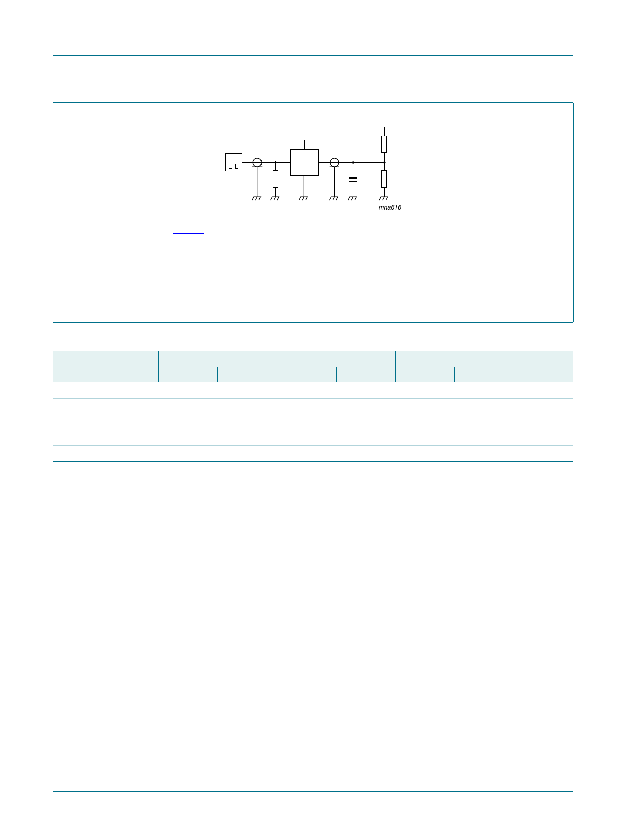
VI
G
VCC
VO
DUT
RT
VEXT
RL
CL
RL
mna616
Fig 9.
Test data is given in Table 10.
Definitions for test circuit:
RL = Load resistance.
CL = Load capacitance including jig and probe capacitance.
RT = Termination resistance should be equal to output impedance Zo of the pulse generator.
VEXT = External voltage for measuring switching times.
Load circuitry for switching times
Table 10. Test data
Supply voltage
VCC
1.65 V to 1.95 V
2.3 V to 2.7 V
2.7 V
3.0 V to 3.6 V
4.5 V to 5.5 V
Input
VI
VCC
VCC
2.7 V
2.7 V
VCC
tr, tf
≤ 2.0 ns
≤ 2.0 ns
≤ 2.5 ns
≤ 2.5 ns
≤ 2.5 ns
Load
CL
30 pF
30 pF
50 pF
50 pF
50 pF
RL
1 kΩ
500 Ω
500 Ω
500 Ω
500 Ω
VEXT
tPLH, tPHL
open
open
open
open
open
tPZH, tPHZ
GND
GND
GND
GND
GND
tPZL, tPLZ
2 × VCC
2 × VCC
6V
6V
2 × VCC
74LVC3G17_6
Product data sheet
Rev. 06 — 6 June 2008
© NXP B.V. 2008. All rights reserved.
8 of 18
Share Link: 