74LVC1G57GF View Datasheet(PDF) - NXP Semiconductors.
Part Name
Description
MFG CO.
74LVC1G57GF Datasheet PDF : 20 Pages
| |||
NXP Semiconductors
74LVC1G57
Low-power configurable multiple function gate
13. Transfer characteristics
Table 12. Transfer characteristics
At recommended operating conditions; voltages are referenced to GND (ground = 0 V).
Symbol Parameter
Conditions
40 C to +85 C
Min
Typ[1]
Max
VT+
positive-going
see Figure 14, Figure 15,
threshold voltage Figure 16 and Figure 17
VCC = 1.8 V
VCC = 2.3 V
VCC = 3.0 V
VCC = 4.5 V
VCC = 5.5 V
VT
negative-going see Figure 14, Figure 15,
threshold voltage Figure 16 and Figure 17
0.70 1.02 1.20
1.11
1.42
1.60
1.50 1.79 2.00
2.16 2.52 2.74
2.61 2.99 3.33
VCC = 1.8 V
VCC = 2.3 V
VCC = 3.0 V
VCC = 4.5 V
VCC = 5.5 V
VH
hysteresis voltage (VT+ VT);
see Figure 14, Figure 15,
Figure 16 and Figure 17
0.30 0.53 0.72
0.58 0.77 1.00
0.80 1.04 1.30
1.21 1.55 1.90
1.45 1.86 2.29
VCC = 1.8 V
VCC = 2.3 V
VCC = 3.0 V
VCC = 4.5 V
VCC = 5.5 V
0.30 0.48 0.62
0.40 0.64 0.80
0.50 0.75 1.00
0.71 0.97 1.20
0.71 1.13 1.40
[1] Typical values are measured at Tamb = 25 C.
40 C to +125 C Unit
Min
Max
0.67 1.20 V
1.08 1.60 V
1.47 2.00 V
2.13 2.74 V
2.58 3.33 V
0.30 0.75 V
0.58 1.03 V
0.80 1.33 V
1.21 1.93 V
1.45 2.32 V
0.23 0.62 V
0.34 0.80 V
0.44 1.00 V
0.65 1.20 V
0.65 1.40 V
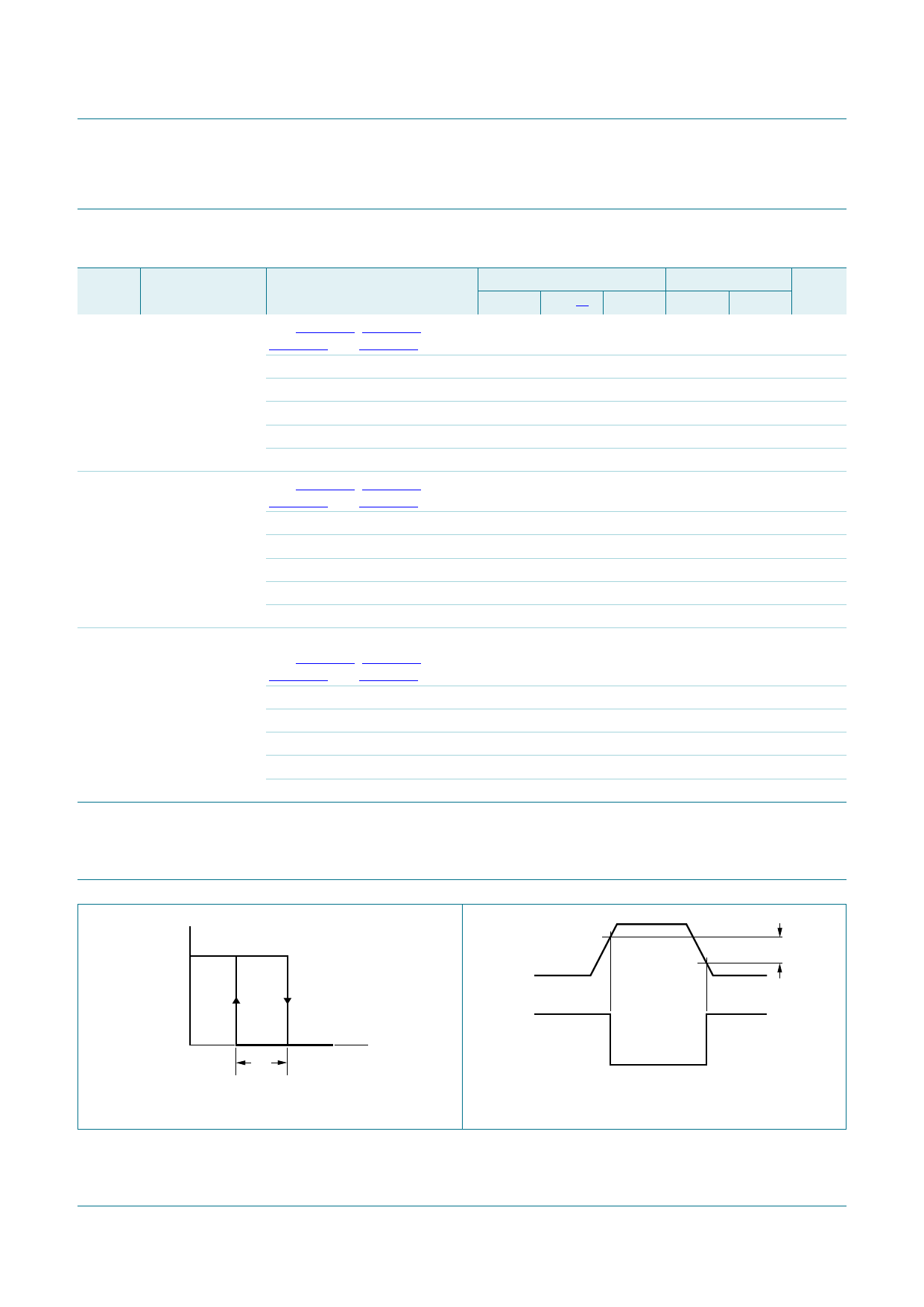
14. Waveforms transfer characteristics
VO
VT+
VI
VH
VT−
VH
VT−
VT+
Fig 14. Transfer characteristic
VI
mna207
VO
mna208
VT+ and VT limits are at 70 % and 20 %.
Fig 15. Definition of VT+, VT and VH
74LVC1G57
Product data sheet
All information provided in this document is subject to legal disclaimers.
Rev. 6 — 6 December 2011
© NXP B.V. 2011. All rights reserved.
9 of 20
Share Link: 